Information Technology Reference
In-Depth Information
TABLE 7.1 Impact of Using Different Organizations
on the Number of Pins
Number of needed
address lines
Number of needed
data lines
Organization
4K
1
12
1
1K
4
10
4
512
8
9
8
256
16
8
16
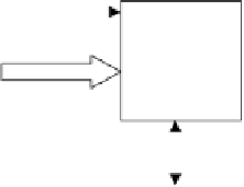
Consider, for example, the design of a 4M bytes main memory subsystem using 1M
bit chip. The number of required chips is 32 chips. It should be noted that the number
of address lines required for the 4M system is 22, while the number of data lines is
8. Figure 7.5 shows a block diagram for both the intended memory subsystem and
the basic building block to be used to construct such a subsystem.
The memory subsystem can be arranged in four rows, each having eight chips. A
schematic of such an arrangement is shown in Figure 7.6. In this figure, the least sig-
nificant 20 address lines A
19
A
0
are used to address any of the basic building block
1M single bit chips. The high-order two address lines A
21
-A
20
are used as inputs to a
2-4 decoder in order to generate four enable lines; each is connected to the CE line
of the eight chips constituting a row.
The above discussion on main memory system design assumes the use of a six-
transistor static random cell. It is possible however to use a one-transistor dynamic
cell. Dynamic memory depends on storing logic values using a capacitor together
with one transistor that acts as a switch. The use of dynamic memory leads to
saving in chip area. However, due to the possibility of decay of the stored values
R/W
R/W
20 address lines
4M bytes memory
System
22 address lines
CE
1 data line
8 data lines
CE
R/W
Mode
0
X
1
0
Tri-state
1
Read
1
Write
X=don't care
Tri-state = high impedance
(a) Intended memory system
(b) Basic memory building block
Figure 7.5 Block diagram of a required memory system and its basic building block


Search WWH ::

Custom Search