Information Technology Reference
In-Depth Information
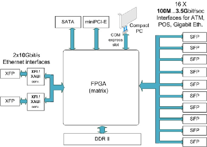
Fig. 1. The simplified structure of the SCALOPES C-board
Each element of this architecture meets the basic dependability
requirements in order to support the overall dependability/survivability of the
system that it is part of.
The main part of the device is the FPGA matrix (or ring), containing four
FPGAs. The FPGA technology helps building a multi-purpose hardware. A
great advantage of this technology is that a simple firmware switch enables us
to switch between applications much faster than if we needed to switch the
whole device.
The outside interfaces (SFP, XFP and COM express slots) connect to the
FPGA's RocketIO ports, which allow high speed communication between
interfaces. The optional variation of interfaces (Gigabit Ethernet optic, 10/100
Ethernet, STM-1 optic etc…) is possible by using SFP module receivers.
The physical and logical connection between the interfaces is defined by
the FPGA firmware ensuring the hardware's flexibility. The current firmware
is physically stored on flash memory connected to the chips: they load as soon
as the hardware starts. I/O data is shared between FPGAs through a dedicated
communication ring interface. There are two rings defined by the clockwise
and counter-clockwise direction of communication, assigned to the two 10
Gigabit Ethernet interfaces.
Fig. 2
depicts the architecture of the board and the
connection of the FPGAs.

Search WWH ::

Custom Search