Biomedical Engineering Reference
In-Depth Information
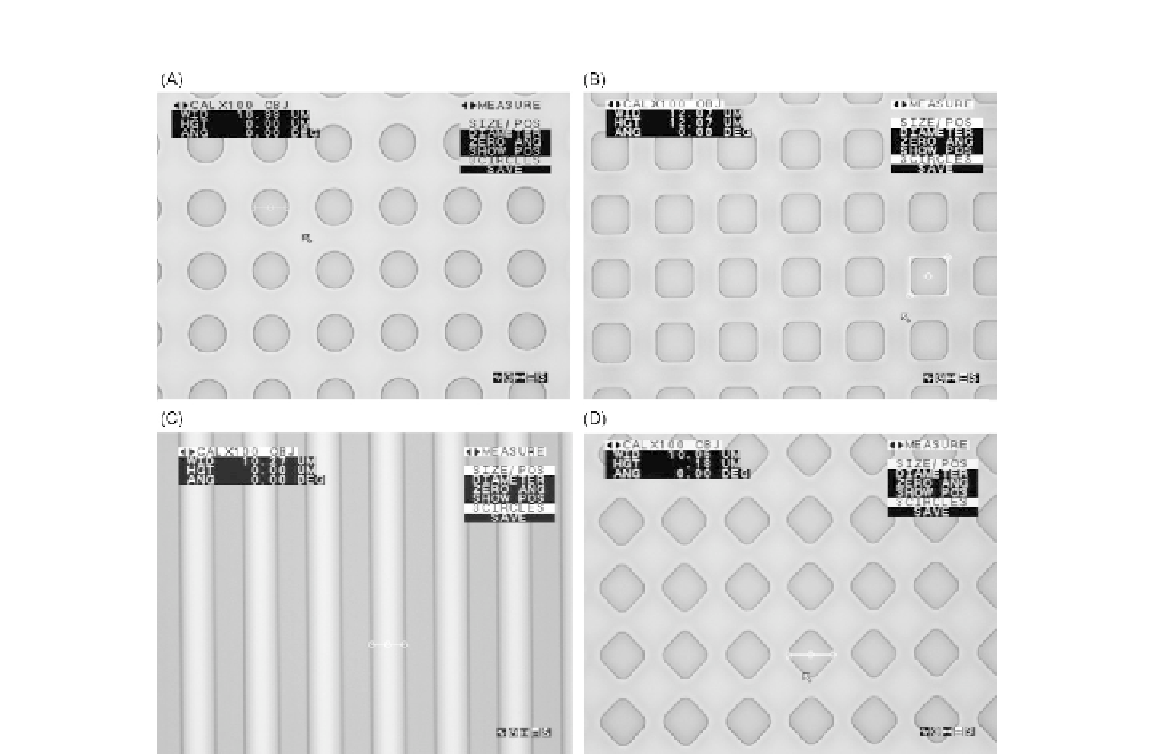
FIGURE 11.4
Reflected light microscopy images of micropatterns of photoresist on silicon wafer (“Master” or negative
mould). All the micropatterns are 10
μ
m in width. The lighter areas are silicon surfaces and the darker
areas are the photoresist micropatterns. (A) Circles, (B) squares, (C) lines, and (D) diamonds.
serves as the photoinitiator which initiates photopolymerization of the PEG-DA molecules on expo-
sure to UV light. This solution was spincoated onto the silanized silicon substrate at 1,000 rpm for
6 s using an EVG101 resist spincoater (Schaerding, Germany). The spincoated uniform layer of the
PEG-DA solution was exposed through the PDMS stamp to UV light (365 nm, 10 mW/cm
2
) for 10 s.
After exposure to UV light, the PDMS stamp was removed. PEG-DA hydrogel micropatterns on the
silicon substrate were developed by immersing the silicon substrates in DI water after 5 min. The
micropatterns were visualized under a light microscope and the dimensions of the fabricated hydro-
gel micropatterns varied from 10 to 40 μm (
Figure 11.9
). Surface profilometry measurements showed
that the depth of the micropatterns ranged between 4 and 10 μm (~7 μm) as shown in
Figure 11.8
.
The cross-linking and photopolymerization of PEG-DA molecules (
Figure 11.6
) is initiated by the
reactive methyl radical from DMPA, the photoinitiator. This methyl radical attacks the double bond