Biomedical Engineering Reference
In-Depth Information
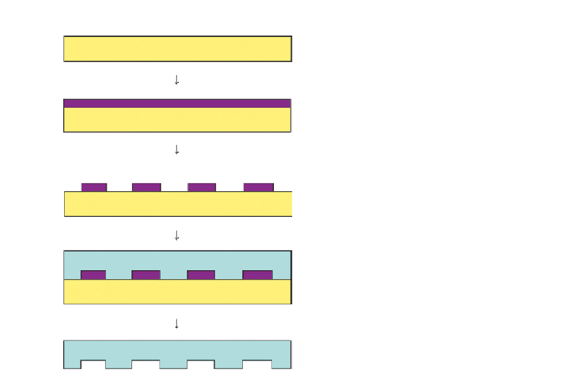
Si wafer
Spincoating of photoresist
Si wafer
Negative mould fabricated by exposure to UV light
through a photomask and developed in a developer solution
Si wafer
PDMS cast over the negative mould
PDMS
Si wafer
PDMS stamp removed from the mould
PDMS
FIGURE 11.3
Schematic illustrations of procedures done for the
fabrication of PDMS stamp.
protective safety clothing were used while handling the piranha solution. After 10 min the silicon sub-
strates were removed from the piranha solution and thoroughly rinsed with deionized (DI) water and
dried under nitrogen. Surface functionalization of the borosilicate glass and silicon substrates with
the silane solution was done by immersing them overnight in 20% (v/v) of TPM and 80% (v/v) of
1,1,1-trichloroethane solution (
Figure 11.5
). The silanized silicon substrates were removed from the
silane solution and rinsed thoroughly with 1,1,1-trichloroethane solution to remove the excess silane
molecules from the silicon substrates and thus ensuring the presence of a silane monolayer. The sili-
con substrates were then dried under nitrogen.
11.5.3
Soft-Photolithography
PEG-DA precursor solution (MW575) was prepared by adding 10 mg of 2,2
-dimethoxy-2-
phenylacetophenone (DMPA) (photoinitiator) to 10 ml of each PEG monomers (1% w/v). DMPA