Biomedical Engineering Reference
In-Depth Information
l
be able to produce many systems simultaneously,
l
be able to structure in three dimensions,
l
be cost-effective.
1.3.1
Top-Down Approach
The most successful industry utilizing the top-down approach is the electronics industry (
Figure 1.2
).
This industry is utilizing techniques involving a range of technologies such as chemical vapor depo-
sition (CVD), physical vapor deposition (PVD), lithography (photolithography, electron beam, and
X-ray lithography), wet and plasma etching, and so on to generate functional structures at the micro-
and nanoscale (
Figure 1.3
). Evolution and development of these technologies have allowed emergence
of numerous electronic products and devices that have enhanced the quality of life throughout the world.
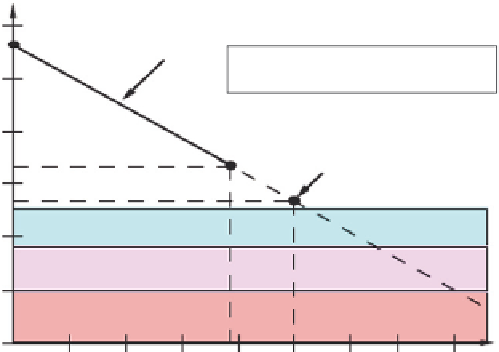
The feature sizes have shrunk continuously from about 75 μm to below 100 nm. This has been achieved
by improvements in deposition technology and more importantly due to the development of lithographic
techniques and equipment such as X-ray lithography and electron beam lithography.
Techniques such as electron beam lithography, X-ray lithography, and ion beam lithography have
advantages in terms of resolution achieved; however, there are disadvantages associated with cost,
“optics,” and detrimental effects on the substrate. These methods are currently under investigation to
improve upon current lithographic process used in the integrated circuits (IC) industry. With continu-
ous developments in these technologies, it is highly likely that the transition from microtechnology to
nanotechnology will generate a whole new generation of exciting products and features.
A demonstration of how several techniques can be combined together to form a “nano” wine glass
(
Figure 1.4
). In this example, a focused ion beam and CVD have been employed to produce this strik-
ing nanostructure.
100
µ
m
Integrated circuit
history
• History and future projections for
minimum feature size in silicon chips.
10
µ
m
1
µ
m
0.25
µ
in 1997
NTRS roadmap
0.1
µ
m
Transition region
10 nm
Quantum devices
1 nm
Atomic dimensions
0.1 nm
1960
1980
2000
2020
2040
Year
FIGURE 1.2
Features size evolution in silicon chips.