Biomedical Engineering Reference
In-Depth Information
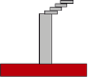
Light
Mask
Photoresist
Deposited film
Substrate
Film deposition
Photoresist application
Exposure
Etch mask
Development
Etching
Resist removal
FIGURE 1.1
A typical process sequence employed in the electronics industry to generate functional devices at the micro-
and nanoscale
[6]
.
Ga focused
ion beam
1
2
3
4
5
Beam scan
direction
Gas inlet
10
−
3
pa
Source gas
Deposited
materials
Substrate
FIGURE 1.2
Demonstration of three-dimensional nanostructure fabrication
[7]
.
1.3.2
Bottom-up approach
The bottom-up approach involves making nanostructures and devices by arranging atom by atom.
The scanning tunneling microscope (STM) has been used to build nanosized atomic features such
as the letters IBM written using xenon atoms on nickel
[8]
(
Figure 1.4
). While this is beautiful and
exciting, it remains that the experiment was carried out under carefully controlled conditions (i.e.,
liquid helium cooling, high vacuum), and it took something like 24 h to get the letters right. Also