Information Technology Reference
In-Depth Information
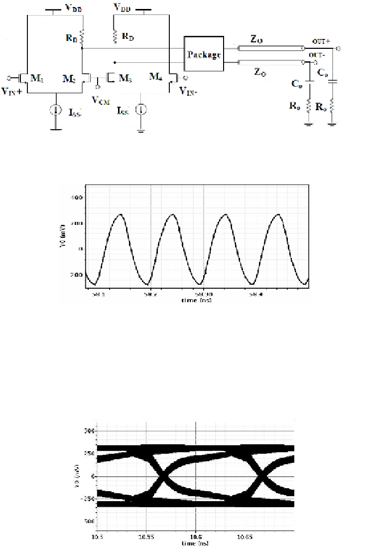
Fig. 5(a).
Complete Schematic of output buffer with package and transmission line output at
offchip load
Fig. 5(b).
Differential Output at off chip load
Table 2.
Rise and Fall times at various point in the system
At Driver
After Package
At off chip load
Rise time (T
r
)
13.82ps
26.45ps
29.4ps
Fall Time (T
f
)
18ps
28.32ps
28.4ps
Fig. 6.
Eye diagram of output for a 10 Gbps pseudo-random bit sequence input