Information Technology Reference
In-Depth Information
Simulation Results
5
The proposed circuit was designed in MOSIS 180nm CMOS technology [5]
and simulated with Cadence Spectre. The supply voltage used was 1.8 V, with a
common-mode dc voltage (V
CM
in Fig. 3) of 1.2 V. At high speed the effect of package
and transmission line parasitics must also be considered for off-chip loads. The
package model was taken from Maxim's 3840 10-Gbps equalizer [6], and the
transmission line model of Spectre was used .
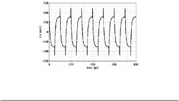
Figure 4 shows the differential output of the buffer before package, for differential
input of 10 GHz. The output shows a differential peak to peak of about 800 mV. Fig
5(b) shows the output of the buffer at offchip load(R
0
C
0
) as shown in Fig5(a)
Table 1 shows the different parameter values obtained from Fig. 4 and Figure 5
shows the output waveform for the same inputs at the off-chip load (includes effect of
package and transmission line) which is 600 mV differential peak to peak.
Table 2 shows the rise and fall times obtained at the driver output, after the package
and at the off-chip load.
Fig. 4.
Differential output at the output of buffer line
Table 1.
Summary of buffer performance at the driver output
Parameter
Value
Rise time (T
r
)
13.82s
Fall Time (T
f
)
V
OH
V
OL
Vswing(single ended)
Power dissipiation
18ps
1.78V
1.39V
0.39V
22.32mW