Information Technology Reference
In-Depth Information
Tabl e 2.
Delay Measurement of 4 different paths of a C880 benchmark circuit
First crossover Second crossover Third crossover
Path Delay
C880 bench.
paths
D1
N1
D2 N2
D3 N3
Using Arch.
Simulation
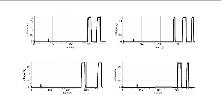
Fig. 9a
304ps 3
90ps 2
12ps 3
756-768ps
761ps
Fig. 9b
304ps 1
90ps 1
12ps 3
238-250ps
246ps
Fig. 9c
304ps 1
90ps 2
12ps 7
196-208ps
207ps
Fig. 9d
304ps 3
90ps 1
12ps 3
846-858ps
854ps
(a)
Scan Out data of Path 1
(b)
Scan Out data of Path 2
(c)
Scan Out data of Path 3
(d)
Scan Out data of Path 4
Fig. 9.
Waveform shows the data obtained at the end of measurement. Measurement
is done by counting number of zeroes and ones starting from the last bit and moving
towards first bit till a third crossover bit is found.
In Table 3 , MVDL and OCDM refers to designs implemented by using the
techniques proposed in [4] and [6], respectively. These designs are implemented
and simulated in SPICE for the purpose of accurate comparison with the pro-
posed work in 180nm and 90nm CMOS technology. We estimated the area of
all designs in Table 3 by measuring the layout area of all the transistors using
SPICE netlist.
Area of OCDM increases due to the use of six buffers in each stage and size
of these buffers increases exponentially with increase in stages. In 90nm CMOS
process, delay of buffer decreases and more number of transistors are required to
make a buffer as compared to buffers in 180nm technology. This is another reason
of increase in area of OCDM as compared to proposed design in 90nm. Estimated
area of the proposed design containing 14 stages, with values of D1,D2 and D3
equals to 300ps, 100ps and 13ps, respectively is reported in Table 3 . Maximum
path delay that can be measured by the proposed architecture is 3900ps, which
is 4.3 times the maximum delay measured by MVDL. In worst case, path delays
upto 900ps can be measured with a precision of 13ps.
Delay difference below DFF setup time was lost in the delay measurement.
To compensate for this loss, a DC compensation unit given in [6], is used in
this design. The design can only measure delay between two rising signals.