Information Technology Reference
In-Depth Information
4.4
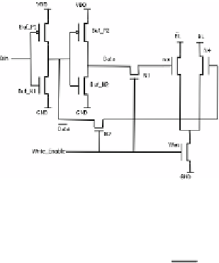
Write Column Circuit
The basic functionality of this circuit is to quickly discharge one of the bit lines from
the precharge level to logic '0'.The circuit is enabled by write signal. For estimating
the leakage current for write circuit, a model has to be designed with the stacked
transistor including transistor N1, N3, N4 and write-enable as shown in figure 7.
In read and idle phase, the write enable signal is off. The bit lines are precharged to
V
dd
in these phases
.
The leakage current contribution is from the buffers and due to the
model that has been characterized priory.
Fig. 6.
Schematic of a Write
Column Circuit [1]
Fig. 7.
Model to analyze leakage current of
write column in idle/read phase
(24)
.
In write phase, the write enable signal is on therefore, the main contributors of
leakage current are the buffers.
. (25)
The leakage current contribution by write column circuit in core memory is,
/
/
.
(26)
.
(27)
Thus, the leakage current of SRAM structure have been estimated as:
.
(28)
5
Results
At first, the curve fitting linear equations for the models have been obtained in the
form,
Ip1 Wp2
Where I is the leakage current, W width of the transistor,
p1 and p2 are the coefficients with following values and with 95% confidence level: