Information Technology Reference
In-Depth Information
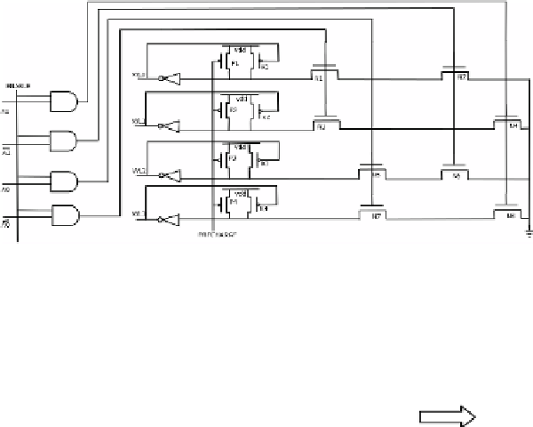
Fig. 2.
Architecture of a 2×4 row decoder
The design includes stacked transistors whose leakage current has been evaluated
using the models shown in Fig. 3,
Stack Model 1 Stack Model 2 Stack Model 3
Fig. 3.
Stack models to analyze leakage current in different modes of row decoder
The third stack model can be replaced by an NMOS in off state, as it results into
same characteristics of leakage current.It maintains the accuracy and also reduces the
time needed to characterise this model.
The leakage current differs with the input at enable and address bits.Based on this
,the lekage current for different input modes are summarised below:
I
INV
I
PMOS
for A0/A1=1 (13)
I
INV
I
NMOS
for A0/A1=0 (14)
I
NAND/STACK
I
MODEL
for vin1, vin2 =00 (15)
I
NAND/STACK
I
MODEL
for vin1, vin2 =10 (16)
I
NAND/STACK
I
NMOS
for vin1, vin2 =01 (17)
I
NAND
2 I
PMOS
for vin1, vin2 =11 (18)
I
STACK
I
PMOS
I
KEEPER PMOS
for vin1, vin2 =11 (19)
Therefore, the leakage current is given by equation (20),
∑
∑
∑
.
(20)