Information Technology Reference
In-Depth Information
delay. Several researchers over the past addressed gate-source/drain underlap. Yang
et
al.
[1] demonstrated the device parameter comparison between overlap and underlap
devices. Bansal
et al.
[2] reported the impact of gate underlap on gate capacitance and
tunneling current. Trivedi
et al.
[3] described the source/drain series resistance and
SCEs optimization for nanoscale underlap FinFETs. Pal
et al.
[4] demonstrated the
dual-
k
spacers that optimize
R
S/D
-
C
fr
tradeoff. This paper primarily focuses on the
complete analysis of underlap length with high-
k
spacers and optimization of underlap
length for superior SRAM's performance.
This research paper is organized into five different sections. Section 2 describes the
device architecture and the simulation setup. In Section 3, we present the electrostat-
ics of underlap FinFET structure and the tradeoffs associated. Thereafter, we analyze
the device characteristics such as drive current, leakage current and their ratio. Sec-
tion 4 incorporates the underlap structure in the SRAM cell. The cell performance is
evaluated based on SNMs (hold, read and write) and the read/write access times. It
also shows the percentage improvement in SRAMs with varying underlap lengths and
different spacer materials. Section 5 finally draws a brief summary.
2
Device Structure and Simulation Setup
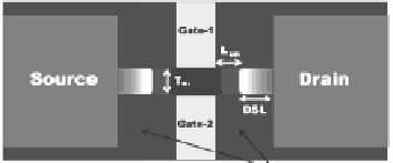
The schematic cross-section of the underlap FinFET structure is shown in Fig. 1. The
device dimensions are calibrated to meet the specification according to ITRS projec-
tions [5] summarized in Table 1. Work-functions of metal gates are tuned to 4.45eV
for n-type and 4.77eV for p-type to achieve the requisite threshold [6]. Source/Drain
extension region uses Gaussian doping profiles followed by a doping gradient of
3nm/decade, such that the dopant-segregation length (DSL) is 12nm. The channel and
underlap regions are lightly doped with boron concentration of 1×10
16
cm
-3
to avoid
random dopant fluctuations while providing high mobility [5]. The gate-electrode
thickness (
T
G
) has kept nearly twice the
L
G
value [1]. Simulations were carried out
with varying underlap length ranging from zero (non-underlap) to 16nm.
Fig. 1.
2D cross-sectional view of the underlap FinFET structure
Synopsys TCAD is used to carry out device and SRAM mixed mode simulations
[7]. The quantum potential model is enabled to include the quantum confinement
effect of inversion carriers in the thin body and also the direct tunneling model is
included to take into account the gate leakages. The Lombardi mobility model has
been activated that account for mobility degradation at the semiconductor-insulator
interface.