Information Technology Reference
In-Depth Information
4
Analysis Methodology and Simulation Environment
Sensing delay is a critical design metric for the nanoscaled memories. All the designs
in comparison with proposed design SA have been optimized extensively and simu-
lated using Cadence Spectre circuit simulator at 45nm technology node, balancing the
trade-off between area, speed and power consumption. Simulation setup is shown in
Fig. 1, with one standard column. The size of the equilibrating device MN4 (Fig. 1) is
kept minimum to ensure retention operation is faster. A standard 6T SRAM memory
cell is used for the simulation. Sensing delay is defined as the difference between the
time when Sense Enable (SAE) is turned on (i.e. SAE=0.5 V
DD
) to the time outB (i.e.
the node that is finally discharged) is reduced to 0.5V
DD
[7], for VMSA. In HMSA
and PDSA delay is equal to the time when CS signal reaches half V
DD
(V
DD
= 0.5) to
the time when the node that is fully discharging reaches half V
DD
. Design is simulated
at various supply voltages and can operate lower down till V
DD
= 0.7V. Fig. 6 plots
sensing delay vs supply voltage at C
BL
=100fF for all topologies and C
BL
=C
DL
=100fF
for HMSA [10] and PDSA. Fig. 7 shows layout of PDSA for area consideration.
Fig.8, shows power consumption vs supply voltage plot, which verifies an 32.86%,
86.32% improvement of the proposed design compared to VMSA and HMSA
respectively.
Fig. 8.
Power dissipation vs. supply voltage
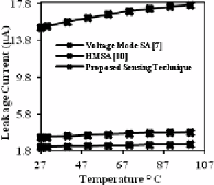
Fig. 9.
Leakage current at various temperature
Table 1.
Comparison with other published work
Sensing
Delay (ps)
Power (µW)
Power Delay
Product (fJ)
Silicon Area
(µ m
2
)
Yield (%)
VMSA[7]
(45nm)
77
3.257
0.2507
3.009
81.6
HMSA[10]
(45 nm)
99.71
16.004
1.5957
12.923
80.3
Proposed
(45nm)
95.32
2.188
0.2085
10.310
100