Information Technology Reference
In-Depth Information
4
Analytical Model
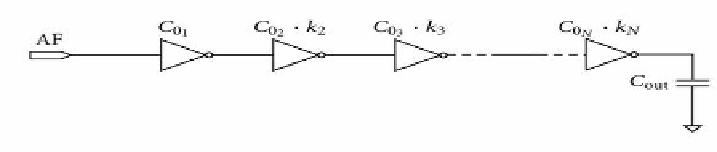
Fig. 6.
Chain of Inverter
From the above section for single stage we found that;
Pgh
(5)
For multiple stage;
PKg
h
g
h
g
h
________________g
N
h
N
(6)
Where 'K' depends upon following factors
•
Supply Voltage
•
Rise time and Fall time of inputs
•
Other MOS parameters like C
ox
and mobility of transistors which depends upon the
model libraries
•
Sub threshold conduction
Further, Initial Energy, E
0
is given as
E
KAF
g
h
AF
g
h
AF
g
h
________________AF
g
N
h
N
(7)
After re-sizing gates by factor 'k
i
' the final energy E
f
comes out to be:
N
E
K
AF
k
g
AF
h
g
k
C
(8)
Where,
•
AF
:activity factor (switching probability) of gate
•
AF
ut
:output activity factor of gate
•
g
:logical effort of gate
•
p
:parasitic delay of gate
•
k
: sizing factor for gate
. The k's are used in the gate re-sizing process
When using the logical effort notation, the initial path delay D
0
is
0
= Σ g
i
h
i
+ P
(9)