Information Technology Reference
In-Depth Information
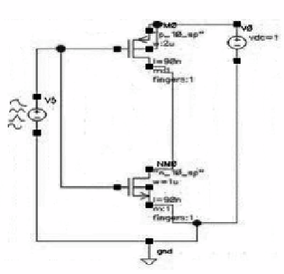
Fig. 2.
CMOS inverter
From fig.2, C
gdp
, C
gdn
are contributing capacitances at input side as well as at the out-
put as in [7], so by using miller effect the capacitance at the input side are;
C
gdp
'= (1+Av)C
gdp
(2)
C
gdn
'= (1+Av)C
gdn
(3)
Here the gain of an inverter (Av) is unity. Theoretically, the total input capacitance is
given by;
C
in
= C
gsp
+ C
gsn
+2C
gdp
+2C
gdn
(4)
Here, we have taken the dimensions of an inverter as Wn=1um, Wp=2um and
L=90nm. The value of oxide thickness was found to be 2.25nm for NMOS and
2.45nm for PMOS for UMC 90nm technology file. Based on oxide thickness values
the oxide capacitance value, which is given by Ɛ
ox
/t
ox
, is calculated for both NMOS
and PMOS respectively. We found for UMC 90nm technology the oxide thickness
values of NMOS and PMOS are found to be 2.25nm and 2.45nm respectively. Hence
we get the oxide capacitances of NMOS and PMOS as:
Coxp = 14.087 mF/m
2
Cox
n
= 15.34 mF/m
2
In order to calculate the input capacitances of an inverter different regions of opera-
tion of an inverter are considered and input capacitances in each case is calculated as
in [7], and the values found are given in the table below: