Information Technology Reference
In-Depth Information
column is faulty. An entire SRAM array is said to be faulty (memory failure) if num-
ber of faulty column is more. A typical memory chip may contain a large number of
sense amplifiers. If some sense amplifiers malfunction then it causes loss of function-
al yield. Hence it is necessary to design robust sense amplifiers that have lower failure
probability against process variations. Sense amplifiers and SRAM cells in particular,
are vulnerable to within-die WID [14].
Frequency of incorrect samples
P(failure) =
×
100 (1)
Total number of inter-die Monte Carlo samples
To estimate the yield of an SA design, Monte Carlo simulations for inter-die distri-
butions of V
th
(assumed to be Gaussian) need to be performed.
Proper sizing of the SA transistors can reduce the failure (due to within-die varia-
tion) probability of a cell at nominal inter-die corner. To understand this, we applied a
certain amount of V
th
shift to all the transistors in an SA (represents an inter-die V
th
shift). To reduce the probability of sensing failure, NMOS transistors (MN3, MN5)
are slightly upsized in the proposed design. The upsizing of NMOS transistors lower
the trip point voltage that flips the cross-coupled inverters at a lower output voltage.
Symmetric layout is a critical piece of our design strategy to reduce mismatch in bit-
line and data-line capacitances, which reduces the probability of sensing failure and
increases yield.
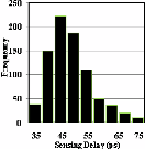
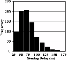
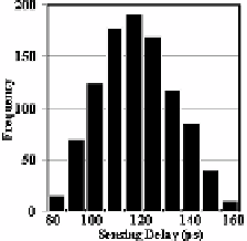
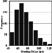
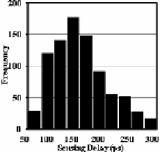
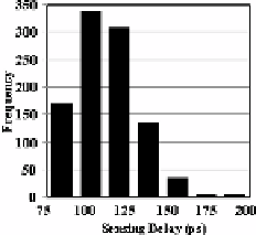
Post layout circuit characteristic with inter-die variation, obtained by
Monte Carlo simulation of 1000 iterations with 3
σ
parameter variation are shown in
μ = 116.567p
V
= 16.7052p
npass = 1000
μ = 69.8003p
V
= 27.4688p
npass = 803
μ = 47.1699p
V
= 6.76773p
npass = 816
(a) Voltage mode SA at V
DD
=1V (b) HMSA at V
DD
=1V (c) Proposed sensing technique at V
DD
=1V
μ = 144.334p
V
= 54.9918p
npass = 862
μ = 108.084p
V
= 14.8665p
npass = 1000
μ = 62.9677p
V
= 14.6082p
npass = 796
(b) HMSA at V
DD
=0.9V (c) Proposed sensing
technique at V
DD
=0.9V
(a) Voltage mode SA at V
DD
=0.9V
Fig. 4.
Sensing Delay histogram of the designs in comparison , results are from 1000 sample
Monte Carlo simulation that vary local parameters (3˃) at room temperature and
C
BL
=C
DL
=100fF