Information Technology Reference
In-Depth Information
By using the current-voltage characteristic of a MOS transistor and neglecting the
channel length modulation effect, the value of reference voltage is given as
(
)
K
W
L
2
I
0
V
=
V
+
1
+
M
21
−
M
12
.
(5)
(
)
REF
th
K
W
L
K
+
K
M
23
M
21
M
12
M
13
Where Ki = µ
i
.C
ox
, V
th
= |V
thM23
| + V
thM21
- V
thM13
,
µ
is the mobility of electron in the
channel, Cox is the oxide capacitance per unit area, V
th
is the threshold voltage, and
W and L are the channel width and length respectively [5].
3
Simulation and Results
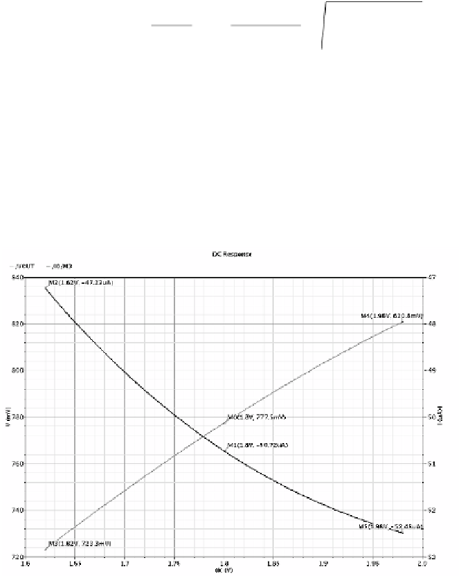
The proposed combined reference circuit is implemented in 0.18 µm CMOS 1.8 V
technology. Fig. 2 and Fig. 3 show the characteristics of current and voltage reference
for supply variation from 1.62 to 1.98 V for Pre and Post simulation.
Fig. 2.
Pre-Simulated behavior of the Combined Reference with Supply Variation
The Pre-Simulation average supply dependency for current is 285 ppm/V and for
voltage is 348 ppm/V, while for Post-Simulation average supply dependency for current
is 285 ppm/V and for voltage is 347 ppm/V. Fig. 4 and Fig. 5 show the Pre and Post
Simulation results for current and voltage reference, while temperature ranges from
−
40
°
C to 125
°
C. The Pre-Simulation average temperature coefficients are 98 ppm/
°
C and
293 ppm/
C for current and voltage generator respectively, while for Post-Simulation
average temperature coefficients are 93 ppm/
°
C for current and voltage
generator. Fig. 6 shows the layout of the proposed Combined Reference Circuit.
°
C and 295 ppm/
°