Information Technology Reference
In-Depth Information
1.0
BL
0.8
EQ
Out
BLB
0.6
CDL
CS
Out
OutB
Pre
PREG
WL
CDLB
BL
B
WL
0.4
OutB
0.2
0.0
3.5
3.75
4.0
4.25
4.5
4.75
5.0
Time (ns)
Fig. 2.
Simulated voltage at various nodes
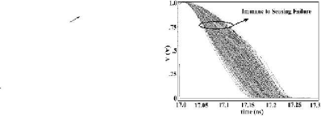
Fig. 3.
Output characteristic for V
th
distribution
(CS) lines are being activated during the read cycle, upper memory cell in the column
will be selected and start drawing current 'I
cell
'. Since drains of MP4 and MP5 are
already near GND potential, once CS signal goes low MP4 and MP5 are driven to
saturation. Since all the devices of CMC (MP2-MP5) are equally sized to ensure satu-
ration mode of operation, MP2 and MP3 will also operate in saturation. We up size
the CMC devices to reduce the effect of process variation, reducing the delay until
self loading dominates. CMC offers very less input resistance to the bit-lines and
instantaneously transfer currents I
L
' and I
R,
without waiting for the discharge of bit-
line capacitances to current transporting data-lines (DLs). Here I
L
'=(I
L
+I
CBL
) and
(I
R
=I
L
+I
CBL
-I
cell
), hence left hand side passes more current, I
L
'>I
R,
and charge the data-
line capacitances producing differential voltage at the source terminal of the NMOS
devices (MN3 & MN5) of the cross coupled inverters. Thereafter, Sense Enable Sig-
nal (SAEN) goes low and EQ signal is deasserted, turning device MP6 on and MN4
off respectively, and cross coupled inverter quickly finishes the latching process pull-
ing node X3 to V
DD
while node X4 is discharged to near ground. Two inverters are
designed here to drive large loads and provide full logic swing at the output. Since no
differential discharging of capacitance is required to sense the cell data, these signals
propagate almost instantaneously from CMC to the data-lines. Precharge (GND) time
of data-line capacitances through NMOS devices MN1-MN2 is crucial here at near
threshold. The increase in the number of column increases data-line capacitance, in
which case the sizing of MN1-MN2 play a major role to discharge the data-line capa-
citances. Data-line capacitance value also depends on the sizing of PMOS devices in
CMC. Through carefull sizing of the CMC devices we achieved optimum delay. Fig.
2 shows waveform at various nodes of design.
3
Process Mismatch Analysis and Yield Optimization of SA
Random within-die variation in process parameters (principally, V
th
variation due to
random dopant fluctuations) results in different types of parametric failures in an SA.
The parametric failures in SA are principally due to offset
(reduction in the bit-
differential produced while accessing the cell), incorrect flipping of latch in SA while
reading, A column of an SRAM array is defined to be faulty if any of the SA in that