Information Technology Reference
In-Depth Information
2
Device Structure and Simulations
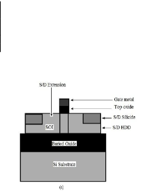
A novel 22nm FinFET was simulated using well calibrated Sentaurus TCAD 3D si-
mulations. The device structure was formed with the aid of Sentaurus Structure Editor
in the TCAD package [10]. Device parameters chosen for simulation are as given in
Table 1. In industry standard <100> Si wafers, mesa etch results in <110> fin side
walls. Since the mobility in <100> plane and <110> plane are different, a double gate
operation has been ensured by keeping a thick oxide layer of 20nm the top surface of
the fin [8]. Hence the structure becomes double gate and the problem of different
current conduction and mobility on two crystallographic planes were solved.
Table 1.
Nomenclature and values of the parameters used in the simulated device
Parameter
Value
Parameter
Value
Gate Length
22nm
Side oxide thickness
1.1nm
Fin Height
40nm
Top oxide thickness
20nm
1E+19 cm
-3
S/D Extension
40nm
S/D extension doping
2 E+20 cm
-3
S/D HDD length
50nm
S/D HDD doping
S/D HDD width
56nm
Gate metal thickness
20nm
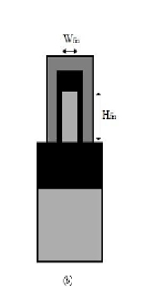
Fig. 1.
FinFET structure used in simulations: (a) cross section along the length of channel and
(b) cross section along the width of the channel
The gate metal work function is selected as 4.5eV and resistivity as 5.44E-6 Ω.cm,
which corresponds to the material properties of Tungsten [9]. To improve the speed of
the device, S/D silicides with resistivity of 2E-6 Ω.cm are employed. In spite of their
positive impact on the speed of the device, silicides provide high temperature stability
and excellent process compatibility with standard Si technology. Heavily doped