Biomedical Engineering Reference
In-Depth Information
(a)
(a)
3
µ
m
20
0 n
m
(b)
(b)
40
Experiment Simulation
Commercial ARC
Si nanopillar array
mc-Si grating
mc-Si wafer
sc-Si wafer
50
30
40
30
20
20
10
10
0
0
400
500
600
700
800
900
1000 1100
400
500
600
700
800
900
Wavelength (nm)
Wavelength (nm)
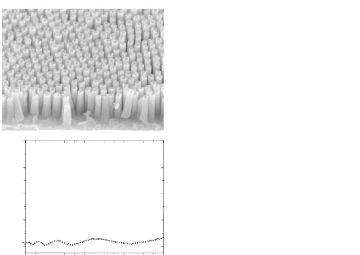
FIGURE 12.14
(a) Cross-sectional SEM image of
20-min-etched silicon nanopillars templated from 70-nm
silica spheres. (b) Experimental and simulated specular
reflection at normal incidence from a commercial single-
crystalline silicon solar cell with SiN
x
ARC, and the tem-
plated silicon nanopillar array as shown in (a). Adapted
from Ref.
106
.
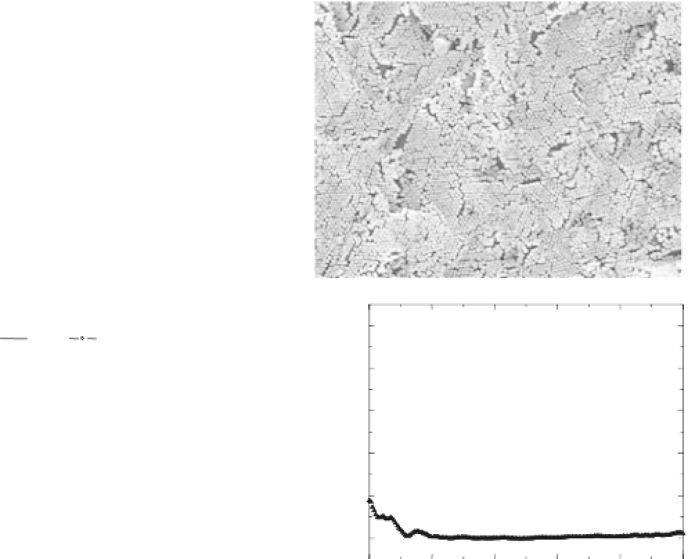
FIGURE 12.15
(a) Typical top-view SEM image of a tem-
plated moth-eye grating on multicrystalline silicon. (b) Com-
parison of hemispherical reflectance obtained from a polished
sc-Si wafer, a commercial mc-Si wafer, and a templated mc-Si
grating. Reprinted with permission from
Appl Phys Lett
99
(2011), 191103. Copyright 2011, American Institute of Physics.
hemispherical reflectance for wavelengths from
400 to 900 nm, matching early measurements in
the literature
[132, 133]
. The rough surface of
the commercial mc-Si facilitates to reduce the
hemispherical reflectance to 20-30%. By con-
trast, the templated mc-Si grating shows excel-
lent broadband antireflection property, and
the hemispherical reflectance is near zero for
a wide range of wavelengths from
∼
500 nm to
∼
850 nm.
12.3.2 Templated Moth-Eye Antireflection
Coatings on Other Semiconductor
Wafers
The templating nanofabrication technology devel-
oped for making moth-eye ARCs on crystalline
silicon substrates can be easily extended to many
other technologically important semiconduc-
tor wafers, such as GaAs and GaSb, which have
been widely utilized in making high-efficiency