Biomedical Engineering Reference
In-Depth Information
+V
IC1
Guard
Ring
In1
Out1
4
J1-1
J2-34
ICxB
In2
Out2
J1-2
J2-1
In3
Out3
5
6
IN-1
J1-3
J2-33
+
7
In4
Out4
OUT-1
J1-4
J2-2
-
IC2
TLC27L4
In1
Out1
11
J1-5
J2-32
In2
Out2
J1-6
J2-3
In3
Out3
J1-7
J2-31
In4
Out4
J1-8
J2-4
-V
IC3
Guard
Ring
In1
Out1
J1-9
J2-30
In2
Out2
ICxA
J1-10
J2-5
4
In3
Out3
J1-11
J2-29
3
In4
Out4
IN-2
J1-12
J2-6
+
1
OUT-2
2
-
IC4
TLC27L4
In1
Out1
J1-13
J2-29
11
In2
Out2
J1-14
J2-7
In3
Out3
J1-15
J2-27
In4
Out4
J1-16
J2-8
IC5
Guard
Ring
In1
Out1
J1-17
J2-26
In2
Out2
ICxD
J1-18
J2-9
4
In3
Out3
J1-19
J2-25
12
In4
Out4
IN-3
J1-20
J2-10
+
14
OUT-3
13
-
IC6
In1
Out1
TLC27L4
J1-21
J2-24
11
In2
Out2
J1-22
J2-11
In3
Out3
J1-23
J2-23
In4
Out4
J1-24
J2-12
IC7
Guard
Ring
In1
Out1
ICxC
4
J1-25
J2-22
In2
Out2
J1-26
J2-13
10
9
In3
Out3
IN-4
J1-27
J2-21
+
8
In4
Out4
OUT-4
J1-28
J2-14
-
IC8
TLC27L4
11
In1
Out1
J1-29
J2-20
J2-19
In2
Out2
J1-30
J2-15
In3
Out3
J1-31
In4
Out4
J1-32
J2-16
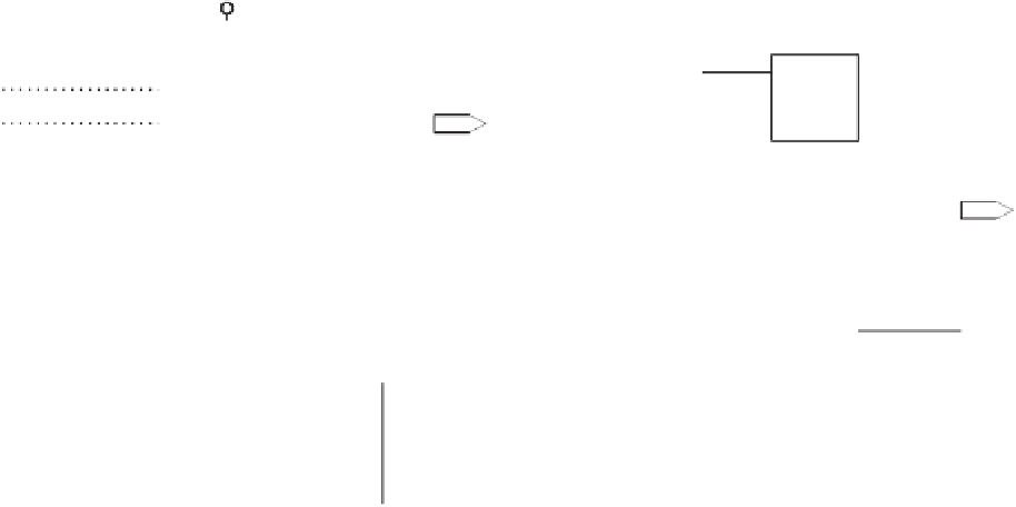
Figure 1.7
ers are often placed in close proximity to high-impedance electrodes to provide impedance con-
version, making it possible to transmit the signal over relatively long distances without picking up noise, despite the fact that the contact
impedance of the electrodes may range into the thousands of megohms.
CMOS-input unity-gain bu
ff
bu
ff
ers, which present an ultrahigh input impedance to an array of up to 32 electrodes. Each
bu
er in the array is implemented using a LinCMOS
1
precision op-amp operated as a unity-
gain voltage follower. An output signal has the same amplitude as that of its corresponding
input. The output impedance is very low, however (in the few kilohm range) and can source or
sink a maximum of 25 mA. As a result of this impedance transformation, the signal at the
bu
ff
er's output can be transmitted over long distances without picking up noise, despite the fact
that the contact impedance of the electrodes may range into the thousands of megohms. Power
for the circuit must be symmetrical
ff
3 to
9 V dc with real or virtual ground.
In the circuit, input signals at J1 are bu
ff
ered by eight TLC27L4 precision quad op-amp.
The bu
ff
ered output is available at J2. Despite its apparent simplicity, the circuit must be
1
LinCMOS is a trademark of Texas Instruments Incorporated.


Search WWH ::

Custom Search