Biomedical Engineering Reference
In-Depth Information
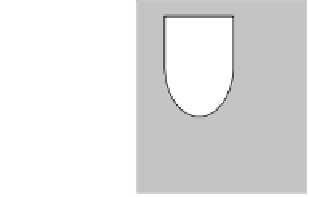
Fig. 2.10
Schematic
configuration of the NW FET
transistor
NW
oxide
S
D
doped semiconductor = gate
immersion of
NWs in ethanol
uniform dispersion of
NWs in ethanol
sonication
pipette
deposition
Fig. 2.11
The deposition steps of NWs between NW FET contacts
Fig. 2.12
The effect of
thermal annealing on the
source-drain I
D
-V
D
characteristic in a Si NW FET
I
D
(μA)
after thermal annealing
4
0
before
-4
V
D
(V)
-1
0
1
In general, the metal contacts of FETs based on NWs are of Schottky types,
and thus, the FET characteristics depend strongly on the contact properties. In Si
NW FETs, however, it was found that thermal annealing and passivation of oxide
defects enhance their performances, which become similar to those of Si MOSFETs
(
Cui et al. 2003
). Si NW FETs are produced using the steps illustrated in Fig.
2.11
,
followed by a 3-min thermal annealing process in hydrogen atmosphere at 600
ı
C.
As a consequence, the mobility and the transconductance of the FET increase 20
times (see Fig.
2.12
).
Many other technologies described in Chap.
1
can be used for the fabrication of
NW devices. For instance, electrodes for NW devices can be produced by room-
temperature nanoimprint lithography, which generates metal features on plastic
substrates. The NWs are deposited afterward on the plastic substrate using the
deposition steps in Fig.
2.11
. This method is used to fabricate many devices,


Search WWH ::

Custom Search