Biomedical Engineering Reference
In-Depth Information
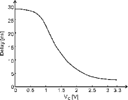
Fig. 8.9
Measured total VCDL delay versus control voltage V
C
out, for the actual operation indeed performs image rejection via back-end digital
signal processing (Sect.
8.2.1
). Using the measured input-referred noise and the
coil impedance (Sect.
8.2.2
), we infer the receiver NF. In the palm system, a
passive gain of 28 offered by the resonance matching (Sect.
8.2.4
)lowersthe
NF from 22.5 to 0.9 dB. In the 1-chip system, a passive gain of 2.1 lowers the
NF from 6.1 to 2.2 dB. The combination of the small input-referred noise and
the resonance matching (optimum noise matching) leads to sufficiently low NF,
making the ping-pong-ball-sized magnet and the lossy on-chip coil viable system
options.
8.3.2
Transmitter Measurements
The measured output impedance of the differential PA (Sect.
8.2.3
) is 27. With the
power supply V
DD
of 3.3 V, the maximum deliverable power at the fundamental
tone is 82 mW. The measured delay versus control voltage, V
C
, of the entire voltage-
controlled delay line (VCDL) in the duty cycle controller (Fig.
8.5
, bottom left) is
shown in Fig.
8.9
. The delay is altered from 29 to 2 ns, as V
C
is varied from 0 to
3.3 V.
The measured duty cycle as a function of V
C
for a 21-MHz excitation signal is
shown in Fig.
8.10
.AsV
C
is changed from 0 to 3.3 V, the duty cycle increases from
0 % to 45 %. This translates to the tuning of output power at the fundamental tone
from 0 to 80 mW (98 % of the total deliverable power of 82 mW).