Biomedical Engineering Reference
In-Depth Information
Fig. 6.11
Nano
structure-based FET
6.3
Signal Transduction Interface
6.3.1
Physically Structured Interface
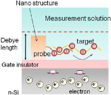
Micro- and nanostructure on gate electrode of semiconductor devices contribute to
increase of surface area for immobilization of probe molecules and amplification of
signals. Nanoparticles or nanopillar can be designed as nanostructure, of which gold,
silica, carbon nanotube, and so on are utilized. In particular, detection limit of FET
devices is closely related to Debye length at the interface between gate surface and
solution. When nanopillar structure is made within Debye length, biomolecules with
longer or larger size such as DNA or protein can be detected within Debye length. In
case of DNA molecules, particularly, more extended DNA molecules based on one
base extension reaction can be detected parallel to gate surface even for longer DNA
molecules (Fig.
6.11
), resulting in label-free DNA sequencing based on intrinsic
molecular charges.
6.3.2
Chemically Synthesized Interface
Functional interfaces synthesized chemically are proposed as monolayer or polymer
membrane. A functional membrane as monolayer sensitive to K
C
at the gate
insulator is prepared using 18-crown-6 ether derivative, as shown in Fig.
6.12
.First,
carboxyethylsilanetriol was used as silane coupling agent. The sensor was immersed
in carboxyethylsilanetriol sodium salt 25 wt% in water for 24 h, then rinsed with
Milli-Q, and dried in a vacuum at 120
ı
C for 1 h. Second, 4-aminobenzo-18-crown-
6 (AB18C6) was used as ionophore of K
C
, and 1-ethyl-3-(3-dimethyaminopropyl)
carbodiimide (EDC) was used as condensation agent. The sensor was immersed in
AB18C6(1mM)andEDC(10mM)inN,N-dimethylformamide (DMF) for 24 h