Biomedical Engineering Reference
In-Depth Information
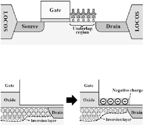
Fig. 5.12
A schematic of an underlap FET. The underlap region is introduced between the gate
and the drain; this region serves as a sensing area
Fig. 5.13
Expanded view of an underlap FET
Fig. 5.14
Bio-experimental
results obtained using an
underlap FET.
Circular dots
indicate the I
V
characteristics of SBP-AIa,
and
square dots
show the
same characteristics for
anti-AI (Copyright 2010
American Institute of
Physics)
of the nanowire and enables the fabrication of perfectly ordered nanowire arrays
[
41
]. Thus, it is timely to consider the structural and/or operational modifications of
nanowire biosensors to overcome the aforementioned challenges while also utilizing
the well-established CMOS technology.
A double-gate nanowire biosensor was proposed to avoid the aggressive scaling
of silicon nanowires in biosensor applications [
42
]. Compared to conventional
nanowire FET biosensors, which are operated using a single bottom gate, the
remarkable difference in the double-gate FET is that independent double gates
(G1 and G2) are positioned vertically beside the silicon nanowire and facing each
other, as shown in Fig.
5.15
.