Biomedical Engineering Reference
In-Depth Information
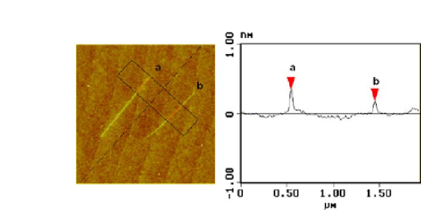
Figure 1.5
AFM image and height profile of two Pt lines drawn at different
scan speed. (a) Line at 10 nm/s and (b) line at 20 nm/s. The voltage applied
at the tip is 3 V for both lines and the relative humidity is 43% [106].
Reproduced by kind permission from the publisher.
Electrochemical AFM “dip-pen'' nanolithography has
significantly expanded the scope where DPN nanofabrication can
be applied. It combines the versatility of electrochemistry with the
simplicity and power of the DPN method to produce nanostructures
with high resolution. Electrochemical STM-based methods require
that the substrates be metallic, but substrates used in EC-DPN do
not have to be metallic since the control feedback of the AFM does
not rely on the current between the tip and surface. Si wafers coated
with native oxide provides enough conductivity for the reduction
of the precursor ions. This development significantly expands the
scope of DPN lithography, making it a more general nanofabrication
technique that not only can be used to deliver organic molecules
to surfaces but is also capable of fabricating metallic and
semiconducting structures with precise control over location
and geometry. Local electrochemical deposition of freestanding
vertically grown platinum nanowires was demonstrated with a
similar approach, electrochemical fountain pen nanofabrication (EC-
FPN) [107]. The EC-FPN exploits the meniscus formed between an
electrolyte-filled nanopipette (“the fountain pen”) and a conductive
substrate to serve as a confined electrochemical cell for reducing and
depositing metal ions. Freestanding Pt nanowires were continuously


Search WWH ::

Custom Search