Information Technology Reference
In-Depth Information
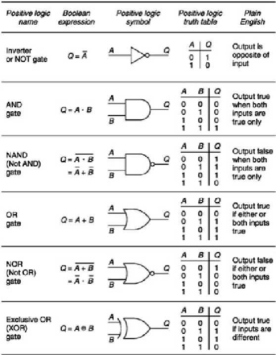
Figure 2.31:
The basic logic gates compared.
If numerical quantities need to be conveyed down the two-state signal paths described here, then the only
appropriate numbering system is binary, which has only two symbols, 0 and 1. Just as positive or negative logic
could be used for the truth of a logical binary signal, it can also be used for a numerical binary signal. Normally, a
high voltage level will represent a binary 1 and a low voltage will represent a binary 0, described as a 'high for a
one' system. Clearly a 'low for a one' system is just as feasible. Decimal numbers have several columns, each of
which represents a different power of ten; in binary the column position specifies the power of two.
Several binary digits or bits are needed to express the value of a binary sample. These bits can be conveyed at the
same time by several signals to form a parallel system, which is most convenient inside equipment or for short
distances because it is inexpensive, or one at a time down a single signal path, which is more complex, but
convenient for cables between pieces of equipment because the connectors require fewer pins. When a binary
system is used to convey numbers in this way, it can be called a digital system.
2.16 Storage elements
The basic memory element in logic circuits is the latch, which is constructed from two gates as shown in
Figure
2.32
(a), and which can be set or reset. A more useful variant is the D-type latch shown at (b) which remembers the
state of the input at the time a separate clock either changes state, for an edge-triggered device, or after it goes
false, for a level-triggered device. A shift register can be made from a series of latches by connecting the Q output
of one latch to the D input of the next and connecting all the clock inputs in parallel. Data are delayed by the
number of stages in the register. Shift registers are also useful for converting between serial and parallel data
formats.
Where large numbers of bits are to be stored, cross-coupled latches are less suitable because they are more
complicated to fabricate inside integrated circuits than dynamic memory, and consume more current.
In large random access memories (RAMs), the data bits are stored as the presence or absence of charge in a tiny
capacitor as shown in
Figure 2.32
(c). The capacitor is formed by a metal electrode, insulated by a layer of silicon
dioxide from a semiconductor substrate, hence the term MOS (metal oxide semiconductor). The charge will suffer
leakage, and the value would become indeterminate after a few milliseconds. Where the delay needed is less than
this, decay is of no consequence, as data will be read out before they have had a chance to decay. Where longer
delays are necessary, such memories must be refreshed periodically by reading the bit value and writing it back to
the same place. Most modern MOS RAM chips have suitable circuitry built in. Large RAMs store many megabits,
and it is clearly impractical to have a connection to each one. Instead, the desired bit has to be addressed before it