Hardware Reference
In-Depth Information
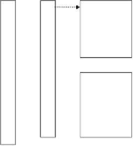
Cell control bus
Operation cell control / Configuration control
MAC
Multiplication/
Mult. & accm./
Accumulation/
Addition
From four
neighboring
cells
To four
neighboring
cells
THR
Data control
×
4
×
4
1-bit data (carry) with a valid bit
8-bit data with a valid bit
Fig. 3.50
Block diagram of multiplication (MLT) cell
multiply-accumulation, accumulation, and addition and a THR unit executing data
controls. The configuration control circuits include configuration registers that store
configuration data corresponding to CPU commands, which determines the opera-
tion of the cell. Each cell can execute as many as four operations at the same time,
and the number of cycles consumed varies from one to three depending on its opera-
tion. Table
3.12
lists the instruction set, which includes 49 instructions for the ALU
and MLT cells. The instructions support data widths of 16 bits, 8 bits, and 1 bit,
where no suffix is attached to instructions for 16-bit data, suffix “.B” is attached for
8-bit data, and suffix “.C” is attached for 1-bit data.
3.2.3
Memory Blocks and Internal Network
The FE-GA has a 10-bank local memory (CRAMs) in order to store both operands for
the operation cell array and operation results. Each bank can be accessed from both the
operation cell array and the outside CPUs in a unit of 16-bit data. The maximum size
of a memory bank is 16 KB or 8 K words. The bank is a dual-port type; therefore, both
data transfers to/from the memory and operations on the cell array can be executed
simultaneously.
To utilize multiple banks of the local memory easily and flexibly, it has load-
store (LS) cells that can be configured exclusively for access control of every bank.
Figure
3.51
shows a block diagram of the LS cell. The LS cells generate addresses,


Search WWH ::

Custom Search