Hardware Reference
In-Depth Information
CLK0
CLK0_0
Module A
Module A
Clock Buffer
CLK0_1
CLK1
Clock Gating Cell
Module B
Module B
CLK1
CLK2
Module C
CLK2
Module C
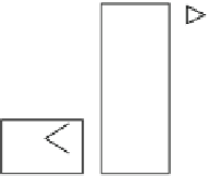
(i) Conventional Clock Tree
(ii) after Power Optimization
Fig. 4.26
Power optimization of global clock tree
Clock
Generator
clock
CK, /CK
F/F
CMD,ADDR.,DM
CMD,ADDR.,DQM
Write Data
F/F
DQ
Read Data
F/F
F/F
90°
Shift
Mask
Logic
FIFO
DQS
F/F
PHY
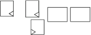
Fig. 4.27
DDR3-SDRAM interface
the Module C is not used. In a large-scale chip, it is not easy to lay out all the mod-
ules using the same clock close together, and proper tree separation is effective for
reducing the power. A gate-level simulation showed that by applying this method,
the deactivation of all clock buffers related to MX-2 and PCI-Express saved 41.5 mW
of power at 1.15 V.
4.4.6
Memory Interface Optimization
The RP-X contains two 2-GB DDR3-SDRAM interfaces. Figure
4.27
illustrates the
DDR3-SDRAM interface. The latency of this interface was reduced to improve the
performance and power efficiency by deleting unnecessary data buffering and
invalid data masking. No F/F except retiming F/Fs was used in the DDR3 PHY to
reduce write latency. The DDR3 interface included asynchronous FIFO and invalid
level mask circuit for latching valid strobe signals from a bidirectional interface to
reduce read latency. Overall, the DDR3 interface including I/O buffer and data sam-
pling requires four cycles (10 ns), and the total latency is nine cycles including
memory latency.


Search WWH ::

Custom Search