Hardware Reference
In-Depth Information
MPC
MPA
Control Registers
Register
Control
Command
SRAM
Data
Instruction
RAM
Control
Logic
FIFO
PEs
Instruction
Fetch
MPA Control
Command
Fig. 3.71
Block diagram of MPC
with data from the XREG and stores the result back to the data register in 1 cycle
with the same way of MX-1. The ALU and XREG operate in parallel when they
access a different bank of the data register. The ALU contains two booth encoders,
an adder, and their peripherals. In MAC operation, a multiplicand data in the XREG
is operated with the outputs of two booth encoders, and they are calculated in the
adder. Therefore, two sets of 4-bit partial product are handled in 1 cycle. 4-bit ALU
calculates partial product four times faster than 2-bit ALU of MX-1, because it
repeats a 2-bit calculations four times.
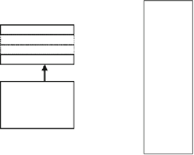
In addition to the improvement of the PEs of MPA, the architecture of MPC is
also enhanced to extract the maximum performance of the parallel processing per-
formance of MX processor. Figure
3.71
shows the block diagram of the MPC. It
basically consists of the instruction RAM, the control registers, and the control
logic. The control logic decodes the microinstructions stored in the instruction RAM
and generates the control command for the control registers in the MPC and PEs
and SRAMs in the MPA. The control registers store the data for controlling the
MPA, such as address pointers. Due to this architecture, when the MPC is occupied
for maintaining the registers in itself, such as setting the immediate data to the con-
trol registers, the operation rate of the MPA degrades. To avoid this degradation,
FIFO circuits are newly added in the MPC.
Figure
3.72
shows an example operation of the controller and the MPA when an
application program is executed. A1-A4 are instructions for the MPA operation.
C1-C3 are instructions when only the controller is operated and the MPA is not
operated. The MPA needs multiple cycles for A1-A3 instructions. The multiple
cycle execution happens when the same bank of the data register is accessed by
both of the XREG and the ALU in the PE operation. Without FIFO, the controller
must wait for completion of the MPA operation. The MPA also needs to stay in idle
states until A4 instruction in the controller is completed. These “WAIT” and
“IDLE” cycles are absorbed by FIFO. While the MPA executes A1, the controller
can operate without waiting, and the next instructions (A2-A3) are stored in FIFO.


Search WWH ::

Custom Search