Hardware Reference
In-Depth Information
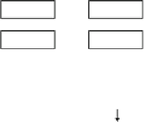
Fig. 3.65
Conceptual
diagram of V-ch operation
Temporary Registers
Entry No.
a[2046]
a[2045]
a[0]
#2046
a[2047]
a[2046]
a[1]
#2047
a[0]
a[2047]
a[2]
#0
a[1]
a[0]
a[3]
#1
a[2]
a[1]
a[4]
#2
a[3]
a[2]
a[5]
#3
a[4]
a[3]
a[6]
#4
a[5]
a[4]
a[7]
#5
initial
+1 entry move
-2 entry move
Intra-bank
V-ch
Inter-bank
V-ch
PE
PE
PE
PE
PE
PE
Bank
#0
Bank
#1
Bank #31
Bank #30
Bank #0
Bank #1
Bank #14
Bank #15
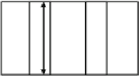
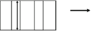
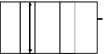
Fig. 3.66
Overview of wire implementations of V-ch
(e.g., +5 entry movement is realized by executing +1 and +4 movement one after
another). Required clock cycles for a movement can be reduced by increasing the
kinds of shift steps; however, those are decided by considering the trade-offs
between the cycle reduction and the area overhead.
Figure
3.66
shows a physical overview of wire implementations of V-ch.
Increasing kinds of shift steps lead to an area overhead; however, V-ch realizes an
area-efficient, powerful network by utilizing its symmetrical layout property and
multi-metal-layer technology. V-ch wire networks are implemented with upper


Search WWH ::

Custom Search