Biology Reference
In-Depth Information
Fabrication of nanophotonic QDWs was achieved using both a
DNA-mediated self-assembly approach and a two-layer molecular
self-assembly procedure based on specific covalent bonds [5,6].
For the DNA process, as depicted in Fig. 12.8, straight and cornered
trenches were patterned on the surface of polymethylmethacrylate
(PMMA) on Si\SiO
using electron-beam lithography.
2
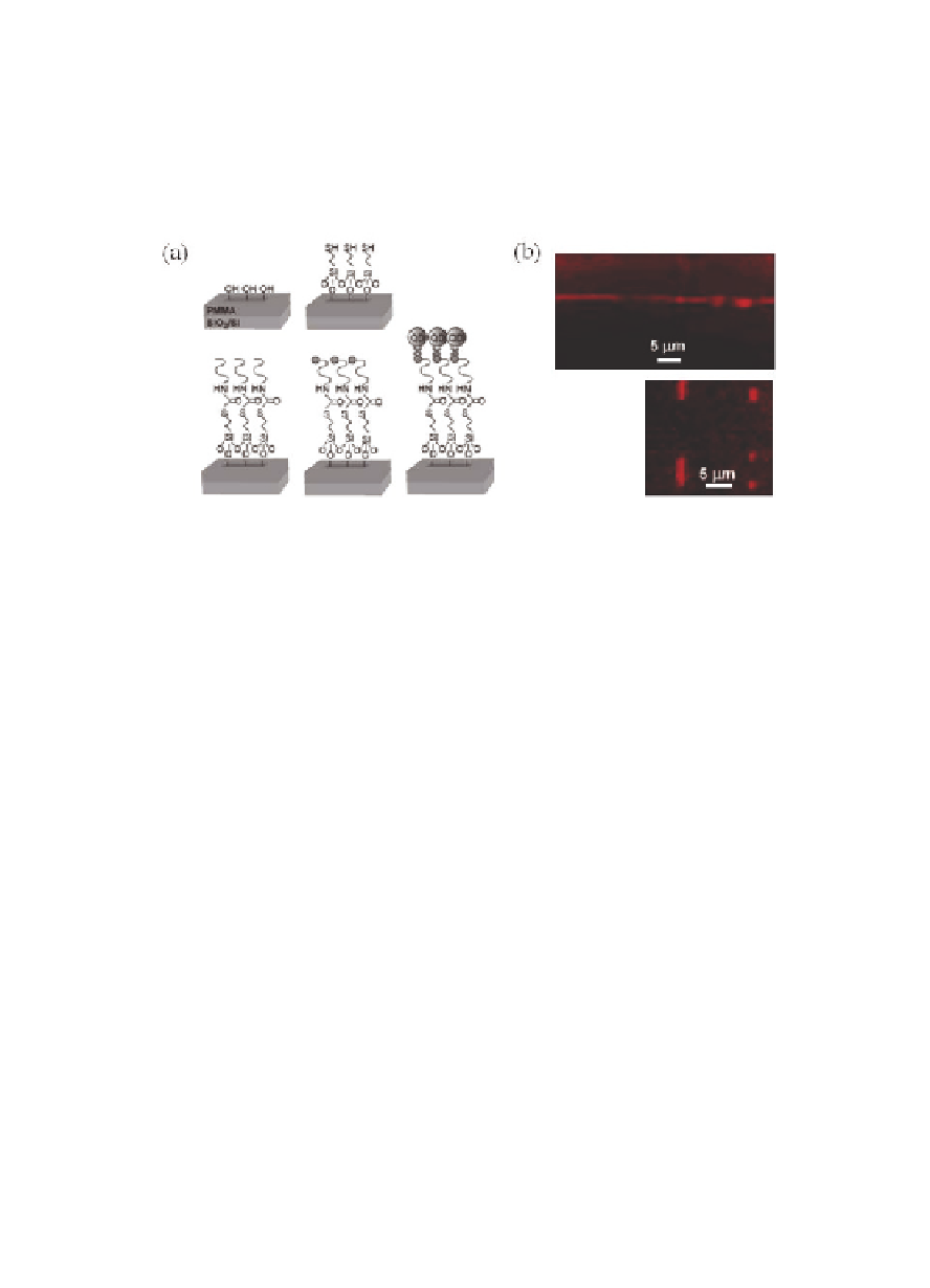
Figure 12.8
QDWs based on DNA-mediated self-assembly of QDs. (a)
Schematic of the self-assembly chemistry. (b) Fluorescence
micrographs confirm QD immobilization as 5
×
1
µ
m
2
, 2
×
m
2
, and 1
m
2
patterns (left), and 1
1
m wide QDWs
(right). Reprinted with permission from Ref. [6]. Copyright
2006 American Chemical Society.
µ
×
1
µ
µ
The trenches define the overall shape of the waveguides. The
Si substrate was chosen to promote integration with existing
circuit technologies. Hydroxyl groups on the SiO
surface act
as anchors for the first assembly step, i.e., the deposition of
3-mercaptopropyltrimethoxysilane (MPTMS) molecules. X-ray
photoelectron spectroscopy (XPS) on the exposed and control
samples confirmed the presence of self-assembled molecular layers
of MPTMS. Acrylamide-modified single-stranded DNA (ss-DNA)
binds specifically to the thiol (SH) termini of the MPTMS molecules
at the bottom of the trenches, thus creating highly specific binding
locations to the exact complementary DNA chain. The binding
specificity of the two complementary DNA strands is utilized to allow
the deposition of QDs in a programmable manner. This is done by
first introducing custom-synthesized biotinylated complementary
DNA (cDNA), followed by streptavidin-conjugated QDs. Finally,
PMMA was removed using a dichloromethane rinse. The QD pattern
remains on the substrate by linking chemistries. DNA assembly
2
Search WWH ::

Custom Search