Biomedical Engineering Reference
In-Depth Information
The output voltage
V
out
is proportional to the integration time
T
INT
and inversely pro-
portional to the feedback capacitor
C
INT
. Therefore, the effective transimpedance gain is
T
INT
/
C
INT
, where very high gain can be achieved by reducing the integration capacitor
values and increasing the integration time. The integrating behavior of this design reduces
noise by averaging noise generated by the photoreceptor, amplifier, and external sources.
The switched integrator design is well matched to the bR photoreceptor because it pro-
vides adjustable gain-bandwidth, low noise, and low power consumption.
17.3.2.2 Analysis of the Switched Integrator
Figure 17.8 shows a more detailed circuit diagram in which a precision switched integra-
tor, IVC102, combines an FET op amp, integrating capacitors, and low-leakage FET
switches onto a single chip. The pixel output connects to the inverting input via a sample
switch S
1
, where the noninverting input is grounded. The reset switch S
2
is in parallel with
the integrating capacitors to provide a discharge path. Amplifier output is connected to a
holding capacitor via a readout switch S
3
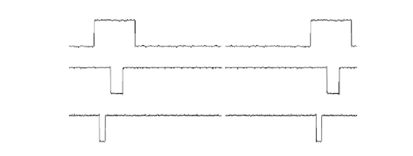
. The overall circuit operates as follows: (1) inte-
gration of the input current begins when S
1
is closed and S
2
and S
3
are opened. Referring
to the timing diagram in Figure 17.9, signal integration occurs over time
a
, where the input
C
1
C
2
C
3
S
2
C
l
R
l
S
1
R
s
S
3
A
2
A
1
+
+
V
out
−
E
ph
(
t
)
C
m
R
m
C
s
IVC102
−
Sample
hold
bR photoreceptor
FIGURE 17.8
Schematic representation of a complete front-end configuration for one bR pixel. Three dashed boxes include the
simplified bR model, IVC102 switched integrator, and sample/hold circuitry.
b
a
S
1
c
e
d
S
2
S
3
f
FIGURE 17.9
Timing diagrams of switches S
1
, S
2
, and S
3
recorded from the microcontroller output.