Biomedical Engineering Reference
In-Depth Information
R
l
C
l
+
R
s
+
V
out
−
+
C
m
R
m
−
E
ph
(
t
)
−
(a)
I
ph
C
l
R
l
R
f
R
s
−
+
−
E
ph
(
t
)
R
m
C
m
V
out
+
−
+
(b)
R
l
C
l
C
INT
R
s
−
+
−
E
ph
(t)
C
m
R
m
V
out
+
−
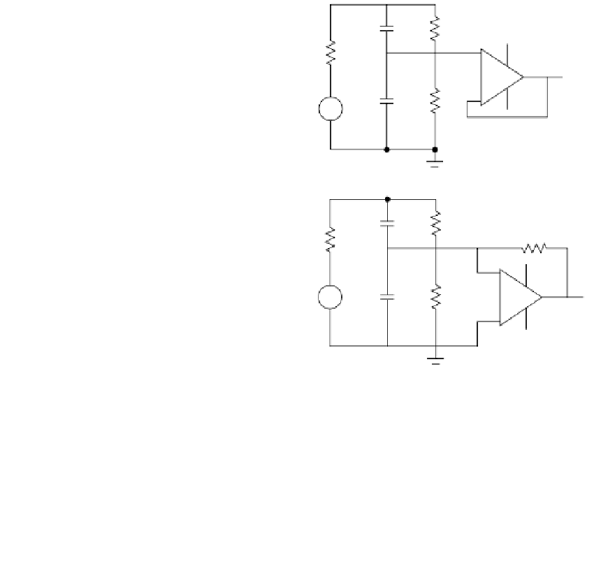
FIGURE 17.7
Schematic representation of simplified equivalent
bR circuit model in combination with three front-
end circuit designs: (a) voltage follower, (b) tran-
simpedance amplifier, and (c) switched integrator.
+
(c)
capacitance
C
m
and resistance
R
m
, thus significantly improving bandwidth. The output
voltage of the transimpedance amplifier is described by
VI
R
(17.5)
out
ph
f
The transimpedance gain is determined by
R
f
. To detect very low signals, a large feed-
back resistor is required (on the order of 1 G
); unfortunately, this approach introduces
system instability and thermal noise.
The switched integrator provides similar functionality to that of the transimpedance
amplifier (Figure 17.7c). It converts an input current into an output voltage, but a capaci-
tor replaces the large resistor in the feedback loop. The input current flows through the
feedback capacitor
C
INT
charging it at a rate proportional to the input current. With an
input current
I
INT
, the voltage at the output is given by
1
∫
V
I
()d
t
t
out
INT
C
INT
(17.6)