Biomedical Engineering Reference
In-Depth Information
15V
R1
15M
C1
100n
13
INA126
R3
820
4
2
15
5
R4
50
OUT
BR element
11
+
12
7
10
C2
100n
R2
15M
15V
(a)
C1
2n
R5
750
OPA132/BB
OPA132/BB
OUT
IN
D2
−
R1 750
2
−
6
2
3
+
6
3
1N4148
R2
R4
750
1.5k
C2
2n
D1
1N4148
RESET
R3
1k
NF5101
(b)
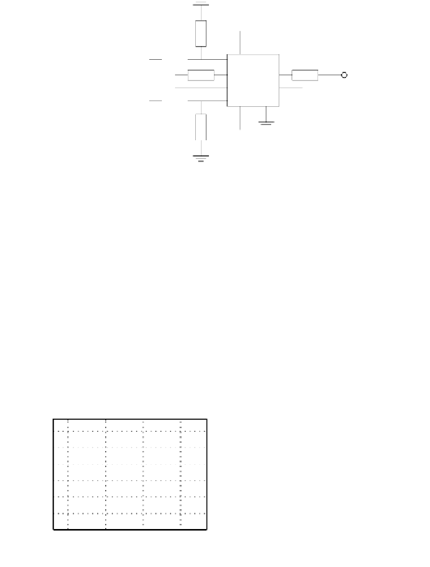
FIGURE 16.10
Electronics for the imaging arrays: (a) the voltage follower and (b) signal amplifier and peak-hold circuitry.
6
5
4
4
3
2
2
1
0
0
0
500
1000
1500
0
50
100
150
Time (ms)
Time (ms)
FIGURE 16.11
Time course of the PER for an element of the gray-scale imaging array. Two time resolutions are used to illustrate
the components in the response.
array element are shown in Figure 16.13. Based on the measurement, the imaging array and
the preparation process cannot be conceived as of industrial quality. However, the preparation
process is straightforward and robust. All prepared photosensors and array elements gener-
ated a PER, and differences between the responses can be compensated using calibration.