Biomedical Engineering Reference
In-Depth Information
1
2
2
1
Time
Time
(A)
S
D
S1
(B)
(C)
Time
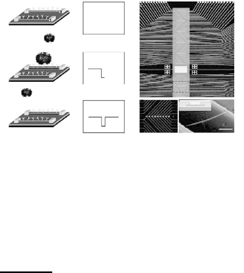
FIGURE 12.26
(See color insert)
Nanowire-based detection of single viruses. Left: Schematic illustration shows two nanowire
devices, 1 and 2, where the nanowires are modified with different antibody receptors. Specific binding of a single
virus to the receptors on nanowire 2 produces a conductance change (middle) characteristic of the surface charge
of the virus only in nanowire 2. When the virus unbinds from the surface, the conductance returns to the baseline
value. Right: nanowire devices and device array. (A) Optical image of the upper portion of a device array. White
lines correspond to metal electrodes that connect to individual nanowire devices. The position of the microfluidic
channel used to deliver sample is highlighted in blue and has a total size of 6 mm
500
m (length
width). The
image field is 4.4
3.5 mm. (B) Optical image of one row of addressable device elements from the region high-
lighted by the red-dashed box in A. The red arrow highlights the position of a device. The image field is 500
400
m. (C) Scanning electron microscopic image of one silicon nanowire device. The electrode contacts are visible at
the upper right and lower left regions of the image. (Scale bar: 500 nm.) (
Inset
) Cross-sectional schematic illustra-
tion of a single silicon nanowire device. The nanowire (orange horizontal line) is connected at its ends by source
(S) and drain (D) metal electrodes (gold), and metal is insulated with a layer of silicon nitride (green). The
microfluidic channel is indicated (blue). Down: selective and multiplexed single virus detection. (From Patolsky,
F., Zheng, G., Hayden, O., Lakadamyali, M., Zhuang, X., Lieber, C. M. (2004). Electrical Detection of Single Viruses.
Proc. Natl. Acad. Sci. U.S.A.,
101, 14017-14022.)
12.6
Conclusion and Future Perspective
Carbon nanotube's and various NW's high electrical conductivity, high aspect ratio,
and unique catalytic properties, combined with their capability for biofunctionaliza-
tion, make 1D nanostructure materials a very appealing nanoscale building block for a
wide range of electronic biosensing applications. The incorporation of nanomaterials
into biosensor systems has expanded rapidly, and will surely result in further impres-
sive advances. This chapter has presented detailed information about processing tech-
niques to synthesize CNTs and NWs, with emphasis on controlling their
nanostructures. Further, we have summarized recent advances in the applications of
CNTs and NWs to biosensor development during the last decade, involving CNTs and
NWs functionalization, the design of CNTs-based functional electrodes, and the fabri-
cation of FET-based biosensors. In addition, a variety of CNT- and NW-based electronic