Biomedical Engineering Reference
In-Depth Information
electrodes, which act as the source and drain, and the conductance between them can be
measured as a function of gate bias voltage. The recent bloom of nanofabrication tech-
nology and biofunctionalization methods of CNTs has stimulated significant research
interest to develop FET-based nanosensors for monitoring biorecognition events and bio-
catalytic processes. The mechanism of the FET-based biosensor is depicted [173] in
Figure 12.21, where the electrical conductance of the CNT is highly sensitive to the sur-
rounding biological molecules and varies significantly with changes in electrostatic
charges and surface adsorption of various molecules [69]. For example, by judicious
immobilization of a protein-probe layer, it is then a simple matter of monitoring for a
conductance change of the nanotube biosensor to detect a specific binding bioanalyte,
thus obviating the need for prelabeling with fluorescent molecules. FET devices with
nanotubes as the conducting channel are usually fabricated using nanotubes grown by
CVD [16] on top of silicon dioxide from iron NPs with methane/hydrogen gas mixture
at 800
C on doped silicon wafers [81,133,134]. To reduce the contact resistance and
improve the characteristics of the carbon nanotube field-effect transistors (CNTFETs),
electrical leads can be patterned by evaporation and lift-off techniques on top of the nan-
otubes with a small gap between the metallic source and drain, such as Ti, Co, Pt, and
(A)
100 nm
Al
Au
SiO
2
Nanotube
V
sd
Al
2
O
3
I
Nanotube
(B)
V
g
Au
Al
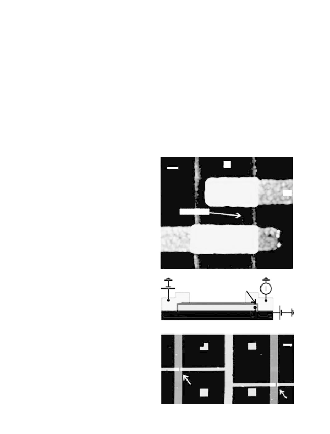
FIGURE 12.21
(See color insert)
Device layout. (A) Height
image of a single-nanotube transistor, acquired
with an atomic force microscope. (B) Schematic
side view of the device. A semiconducting nan-
otube is contacted by two Au electrodes. An Al
wire, covered by a few-nanometers-thick oxide
layer, is used as a gate. (C) Height-mode atomic
force microscope image of two nanotube tran-
sistors connected by a Au interconnect wire. The
arrows indicate the position of the transistors.
Four alignment markers can also be seen. (From
Bachtold, A., Hadley, P., Nakanishi, T., Dekker,
C. (2001). Logic Circuits With Carbon Nanotube
Transistors.
Science,
294(9), 1317-1320.)
SiO
2
(C)
1
µ
m
Al
Au