Biomedical Engineering Reference
In-Depth Information
coworkers [54] have grown Si
3
N
4
, SiC, Ga
2
O
3
, and ZnO NWs by heating the powders of
these materials to elevated temperatures [54]. Wang and coworkers [55] obtained
nanobelts by this method.
12.3.2.2
Solution-Based Growth of Nanowires
12.3.2.2.3 Template-Based Synthesis
Template-directed synthesis provides another class of convenient and versatile methods
for growing 1D nanostructures. In this approach, the template simply serves as a scaffold
within which different materials are synthesized and shaped into a nanostructure with a
morphology complementary to that of the template. The templates could be nanoscale
channels within mesoporous materials, porous alumina, and polycarbonate membranes.
The nanoscale channels are filled using the solution, the sol-gel, or the electrochemical
method. The NWs produced are released from the templates by removal of the host
matrix [56]. Unlike the polymer membranes fabricated by track etching, anodic alumina
membranes (AAMs) containing a hexagonally packed 2D array of cylindrical pores with
a uniform size are prepared by anodization of aluminum foils in an acidic medium
(Figure 12.11). Several materials have been fabricated into NWs using AAMs in the tem-
plating process. NWs of various inorganic materials including Au, Ag, Pt, TiO
2
, MnO
2
,
ZnO, SnO
2
, InO
3
, CdS, CdSe, CdTe, electronically conducting polymers such as polypyr-
role (Ppy), poly(3-methylthiophene), and polyaniline, have been produced, as well as car-
bon nanotubules.
Although the NWs synthesized using the template method are usually polycrystalline,
recent studies have revealed that it is possible to synthesize single crystals of NWs by care-
fully controlled conditions. For example, Takahashi et al. have demonstrated successful
synthesis of single-crystal V205 nonorod arrys by template-based electrodeposition [57].
In recent work, Cao and coworkers [58] discovered that titania NWs obtained from the
electrophoretic deposition method became single crystals once their diameters had been
reduced below 15 nm.
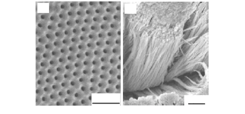
(a)
(b)
300 nm
3
µ
m
FIGURE 12.11
(a) SEM image of AAM template and (b) Bi
2
Te
3
nanowire arrays. (From Jin, C., Xiang, X., Jia, C., Liu, W., Cai, W.,
Yao, L., Li, L. (2004). Electrochemical Fabrication of Large-Area, Ordered Bi
2
Te
3
Nanowire Arrays.
J. Phys. Chem.
B.
, 108, 1844-1847.)