Biomedical Engineering Reference
In-Depth Information
produced by these devices.
10
Importantly, femtomolar sensitivity for DNA was reported,
and the device was also adaptable to the detection of other types of molecular targets. In
the subsequent work, Sailor and coworkers examined reversible binding of immunoglob-
ulin G (IgG) to a PSi surface covalently modified with protein A.
11
Derivatization of the
surface with protein A was found to reduce oxidative degradation of the PSi significantly.
11.3
PSi Biosensors: Early Work at Rochester
In 1999, in collaboration with Philippe Fauchet's research group and initially also in col-
laboration with Prof. Lewis Rothberg, we began to examine the properties of an alterna-
tive device structure in the context of biosensing: the microcavity optical resonator. Such
a device consists of two Bragg mirrors (produced by repeating alternate high- and low-
porosity layers) on either side of a thick “active layer” of PSi (Figure 11.3). This geometry
provides a solution to the observation that controlling the size distribution of the
nanocrystalline silicon structures responsible for the material's luminescence is exceed-
ingly difficult. Instead of the large (>100 nm full width at half maximum (FWHM)) lumi-
nescence bands typically observed with single-layer structures, microcavity resonators
produce luminescence spectra with line widths typically FWHM less than 3 nm. Building
on methods developed for the production of multilayer PSi structures,
12
Fauchet's labora-
tory had initially described the fabrication of PSi microcavity devices in 1999.
13
In that
instance, the microcavity electroluminescence was used to produce what is essentially an
all-PSi light-emitting diode (LED). Importantly, this chapter verified that large changes in
porosity could be effected during the etch process (for highly doped
P
-type silicon wafers)
by changing the current density as a function of time. Since etching only occurs at the
interface between unmodified silicon and the etchant solution, structures remaining
behind are not modified further. This is not necessarily the case for alternative etchant
solutions or alternative substrate materials. Subsequent analysis of the geometry
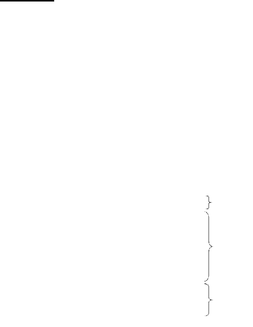
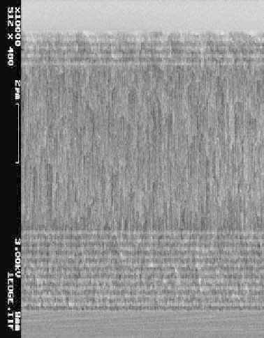
Multilayer mirror
Active layer
FIGURE 11.3
SEM of a porous silicon microcavity.
Note that this particular example is
an asymmetric microcavity (differ-
ent number of mirror periods on
either side of the active layer), which
potentially increases the rate of
diffusion of analytes into the sensor.
Multilayer mirror