Biomedical Engineering Reference
In-Depth Information
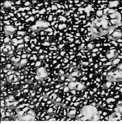
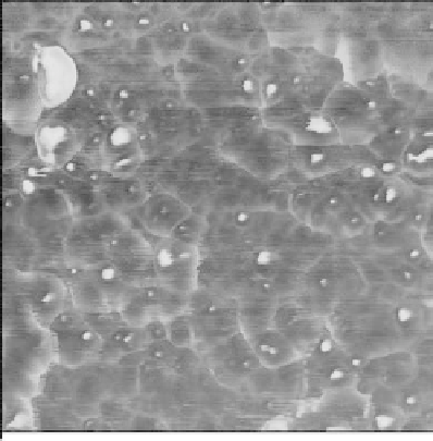
(A)
(B)
0
500 nm
0
500 nm
Data type
Z range
Phase
60.00
Data type
Z range
Phase
60.00
FIGURE 4.11
Atomic force microscopy (AFM) phase images for a 50 nm thick film on an area for (A) PPY and (B) PPY with
entrapped Aqd [59]. (From Ramanathan, K., Bangar, M., Yun, M., Chen, W., Myung, N., Mulchandani, A. (2005).
Bioaffinity sensing using biologically functionalized conducting-polymer nanowire.
J
.
Am
.
Chem
.
Soc
., 127:496-497.
With permission.)
Wang recently reported the functionalization of PPY nanowires with CNTs using a tem-
plate-directed electrochemical synthetic route [61]. PPY was electrodeposited in the pores
of a host membrane in the presence of shortened and carboxylated CNT dopants that
served as charge-balancing counterions. The electron flow within these composite
nanowires was enhanced by the CNTs.
Tao and coworkers [41] incorporated biomolecules in the CP nanojunction using both a
presynthesized monomer-biomolecule conjugate and postpolymerization functionaliza-
tion. In the former, small peptides (gly-gly-his and hexa-his) conjugated to aniline and ani-
line copolymerized to form the nanogap junction while in the latter the enzyme GO
x
was
covalently attached through its lysine -NH
2
to the dopant poly(acrylic acid) -COOH
groups via the condensation reaction.
4.4
Assembly/Fabrication of Nanowire-Based Field Effect Transistor Sensor
Device
The conducting polymer nanowires synthesized in the majority of the techniques presented
above require assembly to fabricate functional sensor device. The most widely used method
of assembling the nanowires into functional sensor device is based on dispersing a dilute sus-
pension of nanowires onto silicon oxide followed by e-beam lithography to form the source
and drain electrodes. An improvement over this random dispersion is the method of fluidic
alignment of the nanowires and then patterning the electrodes by e-beam lithography.
Dielectrophoresis and magnetically assisted assembly are two other powerful techniques that
can be potentially employed for assembling CP NWs into FET sensor devices. We recently
demonstrated assembling, positioning, and spatial manipulating of nanowires by integrating
ferromagnetic ends on nanowires and using the magnetic interaction between ferromagnetic