Information Technology Reference
In-Depth Information
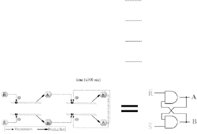
F
igure 4.12
Dynamic behavior and circuit diagrams of the RS latch. The inputs
S
and
R
are normally high and are set to low to toggle the state of the outputs
A
and
B
. The
simulations shows that the gate operates correctly in response to relatively long and
short input pulses.
B
becomes high while
A
becomes low. In a physical implementation of this
circuit, factors such as the relative repression efficiency, original concentration
level, and stochastic noise determine which signal initially becomes high.
After the initial output valu
es
settle into a steady state, an external stimulus
reduces the level of the input
R
to toggle the value stored by the latch. This
relatively long pulse results i
n
expression of the output
A
and a subsequent
decay of the output
B
. When
R
regains its original high level, the circuit still
maintains a high level for
A
and a low level for
B
. Notice that the expression of
A
from two genes during the toggle phase results in a level of
A
that is higher
than than the level of
A
during the steady state following the toggle. However,
the circuit functions correctly because the higher analog value of
A
does not
exceed the range defined to be a digital 1. Because
A
is a repressor, once
A
reaches a saturating repression level, any additional increases in concentration
do not affect the output of the gate.
Finally, a short external stimulus red
u
ces the level of
S
to toggle the RS latch
back to the original state. In this case,
S
regains its high level before
B
builds
up to its own steady-state high level. The level of
B
drops for a short period,