Biomedical Engineering Reference
In-Depth Information
Bulk micromachining:
backside etch
Micromechanical structure
Surface micromachined
structure
Substrate
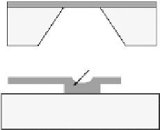
FIGuRE 8.19
Top
:.Bulk.micromachined.wafer.etched.from.the.backside.with.an.anisotropic.etch.that.stops.on.
a.gray.surface.layer..he.gray.surface.layer.can.be.a.dopant.layer.difused.in.from.the.front.side.of.the.wafer.that.
causes.the.anisotropic.etch.to.stop,.or.it.can.be.a.separate.layer,.such.as.the.device.layer.of.an.SOI.wafer..he.back-
side.etch.can.then.stop.on.the.buried.oxide.layer..
Bottom
:.Surface.micromachined.structure..A.micromechanical.
structure.is.formed.from.a.structural.layer,.such.as.polysilicon,.that.is.deposited.on.a.substrate.layer..To.release.the.
micromechanical.structure,.it.can.be.deposited.on.a.patterned.sacriicial.layer,.such.as.an.oxide,.that.is.removed.in.
a.chemical.etch..he.micromechanical.structure.is.attached.to.the.substrate.by.patterning.a.hole.in.the.sacriicial.
layer,.where.the.structural.layer.can.come.into.contact.with.the.substrate.
Two. micromechanical. processes. that. have. been. used. for. fabrication. of. MEMS. DMs. are. bulk. and.
surface.micromachining..Cross.sections.of.these.two.processes.are.shown.in.Figure.8.19..In.bulk.micro-
machining,.the.material.is.removed.from.the.bulk.of.the.wafer.to.leave.behind.the.desired.structure..An.
example.is.a.thin.silicon.membrane.that.can.be.used.as.a.mirror.in.a.membrane.DM..To.obtain.a.thin.
supported.membrane,.the.wafer.can.be.etched.using.an.anisotropic.etch.that.stops.on.a.doped.layer,.as.
shown.by.the.gray.layer.in.Figure.8.19.(top)..Alternatively,.a.silicon-on-insulator.(SOI).wafer.can.be.used.
and.the.etch.stopped.on.the.buried.oxide.layer,.releasing.a.thin.membrane.in.the.SOI.device.layer..he.
wafer.with.the.clamped.membrane.can.be.bonded.with.a.thin.spacer.layer.to.a.second.wafer.that.has.
patterned.electrodes.
8.6.1 Microelectromechanical System Polysilicon Surface
Micromachining Fabrication Process
he. development. of. MEMS. DMs. was. a. major. goal. for. the. NSF. Science. and. Technology. Center. for.
Adaptive.Optics.(CfAO).that.spanned.a.decade.of.research.eforts.from.1999.to.2009.(Krolevitch.2003)..
A. number. of. designs. and. fabrication. methods. were. investigated. including. both. continuous. and. seg-
mented.facesheet.mirrors..Both.designs.used.a.form.of.the.surface.micromachining.fabrication.process,.
so.we.consider.that.process.in.detail.here..By.understanding.the.process,.the.limitations.of.mirrors.fabri-
cated.using.this.process.can.be.better.understood..A.schematic.diagram.of.the.surface.micromachining.
process.is.shown.in.
Figure.8.20
.
he.process.begins.by.deposition.of.a.surface.insulating.material,.enabling.diferent.structures.that.
are.deposited.on.the.substrate.to.be.electrically.insulating..In.
Figure.8.20a
,.silicon.nitride.is.used.as.
the.surface.material..Next.a.spacer.layer.is.deposited.as.shown.in
.
Figure.8.20b
.
.his.layer.is.removed.
at. the. end. of. the. process. to. release. mechanical. components. deined. in. a. structural. material. (poly-
silicon).. In. this. case,. a. phosphosilicate. glass. is. used. because. it. etches. quickly. in. wet. chemical. etch.
(hydroluoric.acid).that.does.not.etch.the.structural.material..he.spacer.layer.is.patterned.to.deine.
an.anchor.area.as.shown.in.
Figure.8.20c
..his.area.will.allow.contact.between.the.structural.material.
and. the. surface. material. on. the. substrate,. enabling. parts. deined. in. the. structural. layer. to. remain.
attached. to. the. substrate. following. the. sacriicial. etch.. In.
Figure. 8.20d
,
. polysilicon. is. deposited. for.
the.structural.material..he.part.of.the.structural.material.that.ills.in.the.anchor.area.etched.through.
the.spacer.material.will.keep.the.released.structural.material.attached.to.the.substrate..he.part.of.the.
structural.material.that.is.deposited.on.the.spacer.material.will.be.released.from.the.substrate.during.