Biomedical Engineering Reference
In-Depth Information
5
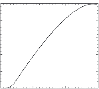
976 nm single VCSEL device
20 deg C, CW
Aperture diameter-300 microns
4
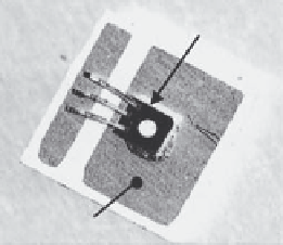
VCSEL die
3
2
1
Princeton optronics-
proprietary & confidential
Submount
0
0
5
10
15
(a)
(b)
Electrical power IN (W)
FIGURE 2.43
(a) 3 Packaged high-power VCSEL device (>2 W). The submount is 2 mm × 2 mm. (b) Shows the
L-I characteristics of a 5 W VCSEL device. The device aperture is 300 u. (Courtesy of Princeton
Optronics [PO] and Dr. Chuni Ghosh. With permission.)
the device mirrors. This coating is a critical processing step for edge emitters,
as any coating imperfection will result in early and catastrophic failure of
the devices due to COD. After this coating step, the wafer strips are diced to
form discrete laser chips, which are then mounted onto carriers. Finally, the
laser devices go into test.
It is also important to understand that VCSELs consume less material: in the
case of a 3″ wafer, a laser manufacturer can build about 15,000 VCSEL devices
or approximately 4,000 edge emitters of similar power levels. In addition to
these advantages, VCSELs demonstrate excellent dynamic performance such
as low threshold current (a few microamperes), low-noise operation, and high-
speed digital modulation (10 Gb/s). Furthermore, although VCSELs have been
typically utilized in low-power applications—a few milliwatts at most—they
have the inherent potential of producing very high powers by processing
large 2-D arrays, as discussed in the section describing high-brightness illu-
mination. In contrast, edge emitters cannot be processed in 2-D arrays.
2.12.3 VCSEL Advantages
The many additional advantages offered by the VCSEL technology can be
summarized in the following points:
1. Wavelength stability: The lasing wavelength in a VCSEL is very sta-
ble, since it is fixed by the short (1- to 1.5-wavelength-thick) Fabry-
Pérot cavity. Contrary to edge emitters, VCSELs can only operate in
a single longitudinal mode.
Search WWH ::

Custom Search