Biomedical Engineering Reference
In-Depth Information
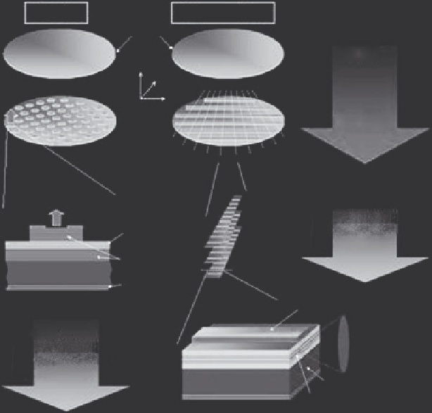
grown wafer is then processed accordingly to produce individual devices.
Figure 2.41 summarizes the differences between VCSEL and edge-emitter
processing.
In a VCSEL, the active layer is sandwiched between two highly reflec-
tive mirrors (dubbed DBRs) made up of several quarter-wavelength-thick
layers of semiconductors of alternating high and low refractive index. The
reflectivity of these mirrors is typically in the range of 99.5%-99.9%. As a
result, the light oscillates
perpendicular
to the layers and escapes through the
top (or bottom) of the device. Current and/or optical confinement is typi-
cally achieved through either selective-oxidation of an aluminum-rich layer,
ion-implantation, or even both for certain applications. The VCSELs can be
designed for “top-emission” (at the epi-air interface) or “bottom-emission”
(through the transparent substrate), in cases where “junction-down” solder-
ing is required for more efficient heat sinking, for example. Figure 2.42 illus-
trates different common types of VCSEL structures.
Edge-emitters
VCSELs
Wafer
Growth
Y
X
Z
Processing
Light output (circular beam)
Active
region
DBR
Edge-emitters:
- Dicing/cleaving
- Additional processing
Substrate
Contact
Contact
Light output
(elliptical beam)
VCSELs:
- Dicing into single
devices, or 1-D or 2-D
arrays
Substrate
Special coating
Active layer
FIGURE 2.41
Comparison of the growth/processing flow of VCSEL and edge-emitter semiconductor lasers.
(Courtesy of Princeton Optronics [PO] and Dr. Chuni Ghosh. With permission.)
Search WWH ::

Custom Search