Biomedical Engineering Reference
In-Depth Information
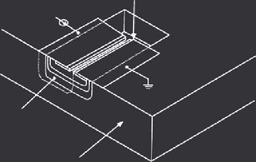
ON-chip
mirror
I
Semi-insulating
GaAs substrate
P
N
Zn
ALGaAs/GaAs DH structure
grown in an etched well
FIGURE 2.28
Schematic representation of the integratable TJS laser grown in an etched well. The on-chip
mirror facet is formed by the undercut mirror process.
lasers having two cleaved mirrors. The optoelectronic chip having a size of
1.8 mm × 1.8 mm operated at speeds up to 150 MHz [71].
More recently, a 1 Gb/s optoelectronic receiver chip was demonstrated [72].
The receiver chip was designed to digitally multiplex four high-speed input
signals. Two of the inputs are electrical and two are optical. The receiver
consisted of two back-to-back Schottky diode detectors, two amplifiers, a 4:1
MUX, and a laser driver. All of the components were fabricated on a semi-
insulating GaAs substrate using direct implantation MESFET technology.
The photodetector was fabricated on a semi-insulating substrate, thus
eliminating the need for epitaxial growth. The pulse response of the back-to-
back Schottky photodiodes [73] had rise and fall times for a range of bias volt-
ages between −10 and −15 V of under 100 ps, which is sufficient for a 1 Gb/s
operation of the receiver. The responsivity of the detector was measured to
be 2.0 A/W for a wavelength of 0.84 μm. The output of the detector is fed
into a three-stage amplifier, a preamplifier, a gain stage, and a buffer stage.
The preamplifier translates the current into a voltage and amplifies to the
proper GaAs logic levels by the gain stage, and the buffer stage is used as a
line driver for the input of the 4:1 MUX. The preamplifier had a gain of 20 dB
with a feedback around the second stage to improve its frequency response.
A similar effort on monolithic integration using a multiple quantum well
(MQW) laser with a ridge channel waveguide structure [74] is shown in
Figure 2.29. The MQW laser structure was grown by MOCVD and consisted
of five 100 GaAs wells separated by four 40 Å Al
0.2
Ga
0.8
As barriers. The ridge
waveguide was ion milled having a width of 5 μm. These integrated devices
Search WWH ::

Custom Search