Biomedical Engineering Reference
In-Depth Information
Wiltron
6659A
sweep
oscillator
IEEE-488 interface bus
Wiltron
560A scaler
network
analyzer
Wiltron
560-98K50
directional
bridge
Rucker &
kolls
1032 wafer
prober
HP 116 12A
bias TEE
HP 116 12A
bias TEE
High
ground
High
ground
DC lines
LTX 77
automatic
test
system
FIGURE 5.31
Typical wafer mapping test station. (After Dammann, C. et al., Microwave die sort and wafer
mapping for GaAs MMIC manufacturing,
Monlithic Technology
, October 1987.)
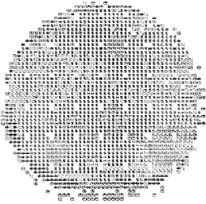
FIGURE 5.32
Typical wafer test station display. @ = high current, # = low current, % = bad rf, & = low gain,
* = high refl, $ = passed.
With this configuration, the operator may run a variety of DC and RF
tests which generate a computer display similar to that [99] depicted in
Figure 5.32. With this information stored in the system controller, the good
dies may be scribed and separated from the unusable. If this prototype
hardware passes testing, the design may go to production. If the design is
flawed, then the design layout, mask generation, and prototype manufac-
turing cycle must be repeated.


Search WWH ::

Custom Search