Biomedical Engineering Reference
In-Depth Information
8 × 10
13
Ar cm
-2
(100) GaAs
100
Annealing of
extended defects
50
Amorphous-to-crystalline
transition (epitaxy)
0
100
200
300
400
500
600
Anneal temperature (°C)
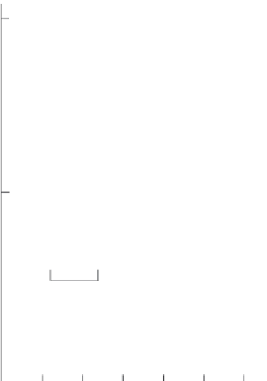
FIGURE 5.24
Normalized disorder, as measured by channeling, for 100 keV 8 × 10
13
Ar cm
−2
-implanted (100)
GaAs plotted as a function of furnace annealing temperature (15 min anneals), indicating
two annealing stages. (From Williams, J.S. and Harrison, H.B., In
Laser and Electron Beam Solid
Interactions and Material Processing
, Gibbons, J.F. et al, eds., North-Holland Publishers, New
York, 1981, p. 209.)
backscattering-channeling spectra, was plotted as a function of the anneal
temperature following an amorphizing implant of 8 × 10
13
Ar cm
−2
at 100 keV.
These data revealed two apparent annealing stages, the first occurring rather
sharply in the temperature range 125°C-230°C (for 15 min anneals), followed
by a second stage in the range of 400°C. Channeling cannot unequivocally
reveal the nature of the residual disorder but, from observations of charac-
teristic color changes during annealing, Williams and others [85] suggested
that stage-1 recovery related to defects corresponding to amorphous regions
in the crystal. Kular [86] correlated channeling, TEM, and electrical measure-
ments, and indicated a third anneal stage in which the density of loops was
progressively reduced.
Of further significance are measurements of electrical activity of ion-
implanted GaAs that show continual improvement up to 9000°C [87]. In
view of the anneal process described, the best electrical behavior is at least


Search WWH ::

Custom Search