Biomedical Engineering Reference
In-Depth Information
n
1
n
1
b
a
c
a
y
n
2
n
2
x
n
3
n
1
n
3
n
5
n
1
n
4
n
4
a
c
a
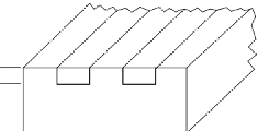
FIGURE 5.13
Parallel channel directional coupler.
of the optical mode profile, it is the interband or band-edge absorption which
will dominate the optical power budget. Purity and control of the fabrica-
tion environment provide both low-loss material (e.g., minimize unwanted
tailing of the absorption band edge), and optimum surface and interference
quality for both efficient electro-optic interaction and maximum optical
throughput.
Intrinsic semiconductor loss is primarily due to free-carrier absorption,
so that selection of the 0.86 μm wavelength is not a disadvantage in terms of
loss relative to 1.3 μm provided the band edge of the optical waveguide rela-
tive to the light source is properly chosen. Losses due to interband absorp-
tion are a serious consideration at 0.86 μm, but with enhanced material
growth and fabrication capability, considerably improved quality materials
(i.e., vastly improved control of defect concentration) will be more readily
available.
The larger amount of waveguiding loss at 0.86 μm can be compensated for
by several approaches. First, at 0.86 a GaAlAs laser diode can be integrated
with other optical components on the same chip to reduce coupling loss. The
required technology to do this at 1.3 μm is considerably lacking. Fabrication
of microwave transistor monolithic integrated circuits and digital integrated
circuits is much farther advanced for GaAs compared to InP. This alone
might suggest the choice of GaAs as a substrate material. Optical amplifiers


Search WWH ::

Custom Search