Biomedical Engineering Reference
In-Depth Information
8
7
N
D
= 2 × 10
17
cm
-3
6
N
D
= 3 × 10
17
cm
-3
5
N
D
= 4 × 10
17
cm
-3
N
D
= 9 × 10
17
cm
-3
N
D
= 10 × 10
17
cm
-3
N
D
= 5 × 10
17
cm
-3
N
D
= 6 × 10
17
cm
-3
N
D
= 7 × 10
17
cm
-3
N
D
= 8 × 10
17
cm
-3
4
3
N
D
= 11 × 10
17
cm
-3
N
D
= 2 × 10
17
cm
-3
2
N
D
= 3 × 10
17
cm
-3
N
D
= 5 × 10
17
cm
-3
N
D
= 8 × 10
17
cm
-3
N
D
= 11 × 10
17
cm
-3
1
0
1
1.5
2
2.5
3
Aspect ratio
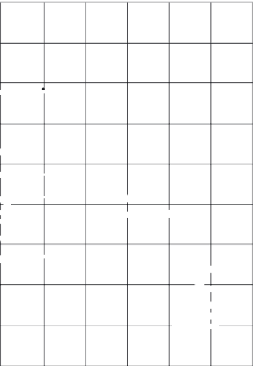
FIGURE 5.12
λ
0
= 10.6 μm—Maximum range of thickness for guiding only the
E E
1
⋅
modes.
x
y
11
and microwave compatibility, and integratability. Much of the work in the
field of optical circuit engineering has involved optimization of a particular
performance aspect. The next step is to realize fully optimized integrated
optical circuit systems.
Of all the considerations involved in the selection of substrate material,
optical loss is often the overriding factor. Optical loss is generally due to arti-
facts of fabrication such as surface roughness, interface strain and defects,
nonideal or non-abrupt dielectric discontinuity, and unwanted interstitial
defect trapping and scattering centers. Aside from optical absorption occur-
ring via free-carrier absorption of power residing in heavily doped regions


Search WWH ::

Custom Search