Biomedical Engineering Reference
In-Depth Information
Wavelength (µm)
10
0.95
0.9
0.85
10
0
0.018 eV
0.036 eV
10
-1
1.50
1.48
1.46
1.44
1.42
1.40
1.38
1.36
1.34
1.32
0.83
295 K
77 K
0.85
0.87
10
-2
0.89
Maximum
Half-power
level
0.91
Resolution
0.93
10
-3
1.24 1.28 1.32 1.40 1.44 1.48 1.52
Photon energy (eV)
100
200
300
(a)
(b)
Temperature (K)
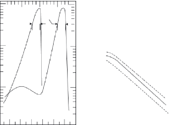
FIGURE 4.18
(a) GaAs diode emission spectra at 300 and 77 K and (b) dependence of emission peak and
half-power width as a function of temperature. (After Carr, W.N.,
IEEE Trans. Electron Devices
ED-12, 531, 1965.)
electrons must be achieved in comparison to the hole electron concentra-
tions at thermal equilibrium. This increased concentration of carriers, also
referred to as an inverted population, can be created in several ways. In the
case of a semiconductor laser diode, the process is referred to as pumping.
In a forward biased p-n junction diode, when holes and electrons recom-
bine in the junction region, photons are generated. The light emitted under
stimulation by the applied forward bias is called electroluminescence. If
light is produced by the injection of photons into the junction region from an
external source, the light emitted by the device is a result of photolumines-
cence. In the case of a light-emitting diode, the light emitted may be heavily
reabsorbed in the bulk material outside the junction. Conversely, the laser
diode is constructed such that absorption in the bulk material is reduced by
making the layer of material between the junction and the external surface
thin, and by choosing a material with as low an absorption coefficient as
possible. The ability of the light source to produce an emission is rated by the
internal and external efficiencies:
number of destred photons emitted
number of electron hole pa
QE
ext
=
irs injected
(4.4)
−


Search WWH ::

Custom Search